The processor included in this console is a slightly customised version of the famous Intel Pentium III (an off-the-shelf CPU for computers) running at 733 MHz. With this, one can assume this console is just a PC behind the scenes... I won't tell you the answer, but I promise that at the end of the article you will be able to reach your own conclusion.
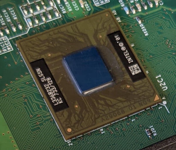
The Intel Pentium III package on the Xbox's motherboard.
Anyhow, Pentiums, along with other lines of CPUs designed and manufactured by Intel, were incredibly popular in the computer market. Such was Intel's market share that they became the de-facto reference point for quality: As a typical user, if you wanted a good computer and had the budget, you only had to look for something carrying an Intel CPU. We all know by now that there are more factors involved, but that's what the marketing guys at Intel managed to project.
Technical information
Now that we positioned Intel on the map, let's go back to the topic of this console. During my research, I was expecting to find documentation with the level of depth as other CPUs (MIPS, SuperH, ARM, etc), but instead, I stumbled across an excessive amount of marketing terms that only diverted my search. So, for this article, I came up with a structure to organise all the necessary information which will help to understand how this CPU works. Furthermore, I will try to introduce some terminology that Intel used to brand this CPU.
Having said that, let us take a look:
Branding
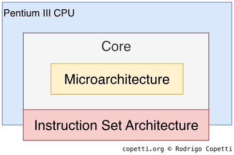
How this study is organised.
First things first, the Xbox's CPU is identified as a Pentium III. So what does this mean? Back then (early noughties), the Pentium series represented the next generation of CPUs. They were the 'new high-end' that grouped all the fancy technology that made computers super-fast, plus it helped buyers decide which CPU they had to buy if they wanted the best of the best.
Pentium III replaced Pentium II, which in turn replaced the original Pentium. Moreover, when the first Pentium came out, it replaced the 80486, which in turn replaced the 80386... You get the idea. What matters is that 'Pentium' is mainly a brand name, it's not directly associated with its inner workings. Therefore, we must go deeper!
To dive further and not get lost in the way, I have catalogued the information into three sections which combined, make up the chip. The first the Instruction Set Architecture or 'ISA' (the group of instructions used to command the CPU), Microarchitecture (how is the ISA implemented in silicon) and the Core (what set of components are used to package the microarchitecture to form the specific CPU model).
The ISA
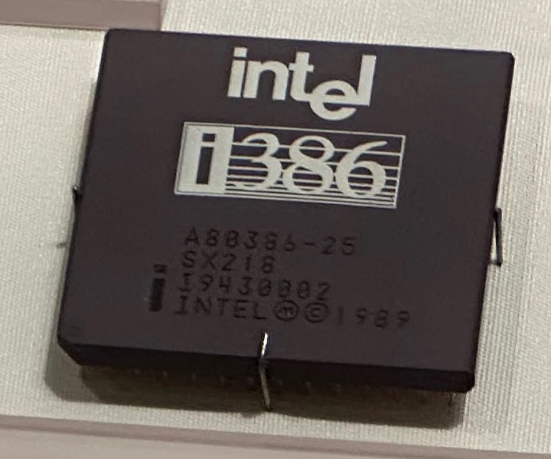
An Intel 80386 (1985), or compatible, was the minimum requirement for mid-90s applications.
Indeed, once I mention 'Intel' it's a matter of time before I introduce the famous x86, its instruction set.
The first form of x86 debuted with the release of the Intel 8086 in 1978, a 16-bit CPU. Afterwards, the ISA was constantly expanded with more instructions as more Intel CPUs were released (80186, 80286 and so on) . Consequently, x86 started to fragment as more ground-breaking features were added (i.e. 'protected mode' and 'long mode'). To tackle this, modern x86 applications commonly target the 80386 ISA (also called IA-32 or i386) as a baseline, which among other things, operates in a 32-bit environment.
Subsequently, Intel enhanced the IA-32 with the use of extensions, meaning the new functions may or may not be included in an IA-32 CPU. Programs query the CPU to check if a specific enhancement is present. The Xbox's CPU includes two extensions:
- MMX (Multimedia Extension): Adds 57 SIMD instructions and 8 64-bit registers (integers only) that can speed up vector operations.
- SSE (Streaming SIMD extension): Another SIMD-type extension that addresses the criticism of MMX (lack of floating-point support and unable to use the floating-point unit in parallel). It adds 56 new instructions and eight 128-bit registers (called 'XMM') that hold four 32-bit
floats.
The good news is that, since the console will always have the same CPU, programmers can optimise their code to exploit these extensions as they will always be present.
The Microarchitecture
When it comes to building a circuit that can interpret x86 instructions, Intel has come up with so many different designs for their CPUs. Some designs were featured with the release of a new Pentium Series (i.e. Pentium 4) while others were featured when Intel released an 'enhanced' version of a Pentium (such as the 'Pentium Pro'). Nevertheless, since the release of the first Pentium, the CPU model and microarchitecture no longer carry the same name. For example, the 80486 uses the 80486 microarchitecture (and no other), however, the original Pentium has the 'P5' microarchitecture.
Now, the Xbox CPU, along with the rest of Pentium III processors, use the P6 Microarchitecture (also known as 'i686'). This is the 6th generation (counting from the 8086) which features:
- A massive 14-stage pipeline: Meaning up to 14 instructions can be processed in parallel. On the other side, individual instructions may take a lot more cycles to complete. See a previous explanation.
- Out-of-order execution: If possible, the CPU re-orders the sequence of instructions to increase efficiency and performance.
- Dynamic execution: Since the P6 is an out-of-order and superscalar design. The traditional branch predictor is now combined with other techniques ('speculative execution' and 'data-flow analysis') to take advantage of the new capabilities. In doing so, it reduces pipeline stalling even further.
Having said that, take a closer look at these features. It so happens they are very similar to previous consoles, however, the other CPUs are very different in terms of design compared to Intel ones. Historically, one could argue that the design of the x86 would've never allowed Intel to produce, let's say, a pipelined CPU. Yet they managed to do so, so let us see why...
CISC or RISC
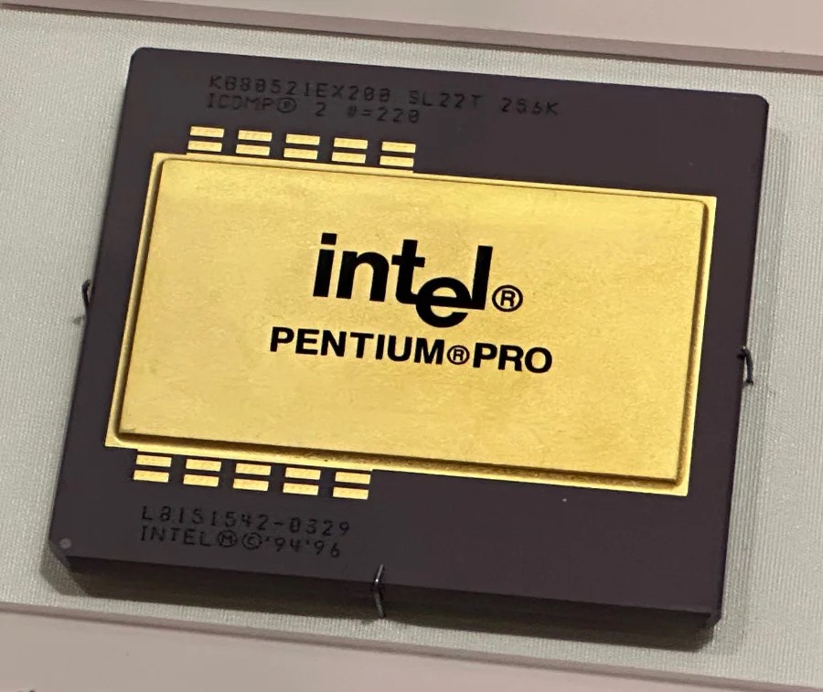
Intel's Pentium Pro (1995) debuted the P6 microarchitecture, bridging the gap between CISC and RISC advancements in the x86 world. This came as a surprise to many - particularly those who believed x86's days were numbered.
The competition happens to feature CPUs designed around the RISC guidelines, whereas Intel's x86 is not, thereby being placed in the CISC group. RISC CPUs are known for having an intentionally simplified design compared to CISC CPUs. This includes, for instance, implementing a load-store architecture, which only provides instructions that operate values from registers (as opposed to operating directly from memory).
One of the advantages of RISC processors is that their simplistic approach enables its CPUs to be designed with a modular sense, which in turn can be exploited to improve performance with parallelism techniques. This is why we have seen CPUs like MIPS and PowerPC debuting pipeline stages, superscalar designs, out-of-order execution, branch prediction, etc. On the other side, CISC processors predate RISC ones and the former aimed to solve different needs. Consequently, their designs are not as flexible as RISC CPUs.
Back to the original question, the P6 is an interesting design, because while this CPU only understands a CISC instruction set (x86), a subset of its opcodes is interpreted using microcode. Most importantly, the unit that executes microcode is built around the load-store model . This is because the P6 architecture was authored by the former engineers of the Intel i960 (a once-promising RISC CPU by Intel). All in all, this has enabled Intel to gain similar advantages to RISC processors without breaking compatibility with the historic x86 ISA. It's fair to say that as time passed by, terms like 'CISC' and 'RISC' have become too ambiguous to categorise any modern CPU.
As a side note, microcode is already embedded in the silicon but it can be patched, allowing Intel to fix its CPUs after production whenever a bug or a security vulnerability is discovered. If you have read previous articles (i.e. N64 or PS2), bear in mind that Intel's microcode is not publicly accessible (let alone documented) and Intel is its sole 'maintainer'.
The Core
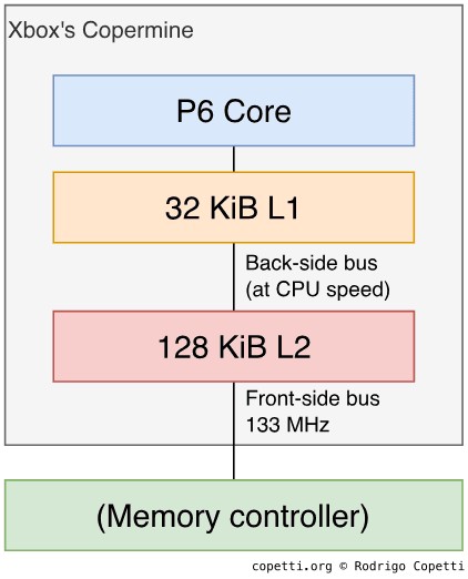
The Coppermine design.
Intel shipped numerous chips that implemented the P6 microarchitecture. The Xbox includes one model called Coppermine. It was branded as the second revision of the Pentium III (replacing the 'Katmai' core) and features the following components:
- 32 KiB L1 cache: Divided between 16 KiB for instructions and 16 KiB for data.
- Integrated 128 KiB L2 cache: This is odd since the off-the-shelf Coppermine has 256 KiB of L2 . In fact, the Coppermine128 (found in the Intel 'Celeron' brand, the low-end Pentium alternative) has the same amount of L2 . Hence, this was probably done to reduce manufacturing costs and keep this console at a competitive price.
- 133 MHz Front-side bus: This is the bus that connects the L2 cache with the memory controller, we'll see more about it later on.
- Intel names it 'Front-side bus' to distinguish it from another bus that connects L2 (external cache) with L1 (internal cache). The latter bus is called 'Back-side bus'... and it's an unfortunate name to use in the UK.
Coppermine also adds two 'enhancements' over their original implementation of L2 cache, these are the Advanced Transfer Cache and the Advanced System Buffering. To sum them up, L2 cache is on-chip and their buses are wider, which helps to reduce possible bottlenecks in the Front-side bus.
Finally, the chip uses the 'Micro-PGA2' socket fit on the motherboard, but like any other console, the Xbox has it soldered with a Ball Grid Array or 'BGA'.
P6 and the end of Pentium numbers
Here's a bit more history. After the years of the P6, Intel planned to succeed it with the 'NetBurst' microarchitecture (featured in the Pentium IV). However, the line of succession also ended there. Even though NetBurst implemented many contemporary techniques , it also suffered from excessive power consumption, heat emission (an average of 85 W ) and scalability issues - all of which impeded the design from being continued any further.
Consequently, this prompted an Intel team in Israel to revisit their low-powered P6 CPU - the 'Pentium M' - and develop a more powerful successor. The first result was the Yonah core, a slight improvement of the P6 design branded as Core Solo or Core Duo. With it, power dissipation dropped to reasonable numbers (between 27 W and 31 W , depending on the variant). Months later, the follow-up Core microarchitecture became the flagship successor of P6 (and NetBurst) and, confusingly enough, reached the shelves in the form of the Core 2 CPU line. Over the years, subsequent microarchitectures improved on many aspects, but they also managed to re-incorporate forgotten elements from NetBurst without repeating the same mistakes.
On a curious note, I wonder if the naming of the Yonah core is meant as a metaphor for the Book of Jonah, particularly connecting the event where the prophet, in the end, managed to correct his path to save the city of Nineveh. Though it's also possible I'm overthinking this.
Motherboard architecture
At some point in the history of the PC, motherboards grew so much in complexity that new designs had to be developed from the ground up to efficiently tackle emerging needs.
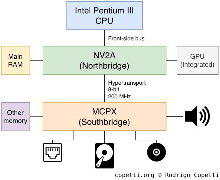
Overview of Xbox Motherboard.
The new standard developed relied on two dedicated chips to handle most of the motherboard functions. These chips are:
- The Northbridge: Serves as a memory controller and interfaces the GPU.
- The Southbridge: Interfaces the rest of I/O (i.e. USB, ATA/SATA, PCI, etc)
The combination of these chips is called chipset and they are important enough to condition the capabilities and performance of a motherboard. The Xbox, being so close to a PC, includes two chips as well: The NV2A, a combination of Northbridge and GPU; and the MCPX which handles the rest of I/O.
Both chips are interconnected using a specialised bus called the HyperTransport. It's worth pointing out that some PC motherboards also included this technology, just with a different brand (nForce MCP-D).
Memory layout
The Xbox includes a total of 64 MiB of DDR SDRAM, this type of RAM is very fast compared to what the competition offers. However, it's also shared across all components of this system. Hence, once more, we find ourselves in front of another unified memory architecture or 'UMA' layout.
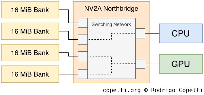
Representation of the switching network. GPU uses two banks while the CPU uses a different one, reducing contention in the process.
We have previously seen how troublesome this design can be sometimes. Nonetheless, programs can address this issue by spreading their data between different banks of memory. NV2A implements a switching network that enables different units (CPU, GPU, etc) to concurrently access them .
Furthermore, the console features an internal hard disk, and it so happens to be set up with three partitions of 750 MiB each reserved for temporary storage. The CPU can offload some of its data from main RAM, then upload it back whenever it's needed. Bear in mind this is a manual process and does not involve virtual RAM.