So while the CPU can be considered a tribute to legacy technologies, let me tell you that the GPU is officially part of the next generation.

Super Mario 3D World (2013).

Hyrule Warriors (2014).

Pikmin 3 (2013).

Splatoon (2015).

The Legend of Zelda: The Wind Waker (2016). Rendered at an exceptional 1920x1080 pixels!
The graphics logic is found within a big silicon chip sitting next to Espresso, it's called Latte, operates at 550 MHz and, to make a long story short, it's broad and complex. Latte houses a lot more infrastructure than just graphics, so don't worry as the former will be explained in the next sections of the article. For now, just remember that the graphics block lives in Latte.

The SoC photo again. So you can contemplate it after being made aware of Latte.
By the way, for the Italian readers, as you may know, the Wii U's codenames are made of terminology related to coffee, and 'Latte' is no exception because that's what non-Italians refer to 'Latte macchiato' :')
Old partnerships with new challenges
Homologous to Nintendo's good relationship with IBM, the company also maintained a unique partnership they started all the way back with the Nintendo 64.
ArtX was the group known for designing the Reality Coprocessor (then as part of Silicon Graphics) which then went on to invent Flipper, the GameCube's unique SoC that houses its signature graphics processor. Years later, after being acquired by 'ATI', they supplied Hollywood for the Wii, from which we find a sped-up version of Flipper's GPU. But most importantly and around the same time, ATI had been working on a cutting-edge invention for Microsoft. The result was Xenos and its new shader model for the masses.
Years after the release of the Xbox 360, ATI got acquired by a silicon company named 'AMD', which brings us to explain a bit of AMD history...
Titans in the ring
Initially known as the sidekick of Intel, AMD used to be the second supplier of Intel's CPUs (i.e. 8086 and 80286), although this relationship broke down as soon as AMD started selling an unauthorised version of the 80386 that, to Intel's dismay, improved upon the original designs of the chip . This didn't sit well with Intel and, soon enough, the two became head-to-head competitors.
Such was the competition, that in the late 90s, Intel's plans to captivate the 64-bit market with their new line of 'Itanium' CPUs were soon thwarted by AMD's simpler alternative: an extension of x86 called 'amd64' (also referred to as 'x86-64'). Thus, Intel was forced to adopt AMD's standard instead. For reference, amd64 still serves as the ISA of current x86 CPUs (as of 2022).
It's never been all jolly for AMD, however. As the pressure from competing with Intel also brought a share of flops out of them (i.e. the abandoned "3DNow!" extension, the delay of Fusion, etc) and now, with the acquisition of ATI in 2006, AMD found itself facing two fronts: Intel in the CPU market and Nvidia on the graphics side.
The next Radeon
Now that we've positioned AMD on the map, let's analyse the state of ATI's Radeon line.
After the introduction of Xenos and its new architecture based on the 'unified shaders' model, ATI was still too busy with Microsoft's project so they couldn't allocate enough resources to bring Xenos to the PC market in the short term. Thus, the remaining teams focused on maintaining their classical x1000/R500 series, which left enough gap for Nvidia to ship their unified card named GeForce 8 (featuring the Tesla architecture) before ATI. Finally, in 2007 (two years after Xenos), ATI presented the Radeon 2000 series (codenamed R600) and its TeraScale architecture. The new design, now free of Microsoft's budget and licensing control, brought all the advancements of Xenos along with optional extras for those users who were willing to pay the premium pricing.
Now, for the Wii U, ATI prepared a Terascale-based card for Nintendo, but it's never been officially confirmed which model they based it on. Fail0verflow relates it to the Radeon HD 4000 series (codenamed R700) . For reference, R700-based cards launched in 2008 and were an incremental update to the R670 and R600 series. The most apparent changes are the inclusion of faster video decoding hardware and support for OpenCL, though only the former will be usable (to some degree) on the Wii U.
In any case, the Wii U's GPU goes by two names, Nintendo calls it GPU7 when referring to the hardware and GX2 when referring to the API. For this article, I'll use the term 'GPU7' as I'll be focusing on the physical capabilities.
Architecture of GPU7
The TeraScale architecture is the materialisation of Xenos/Crayola ported to the PC market... and GPU7 is TeraScale brought back to a console. Its most identifiable trait is the use of a unified shader model that centralises both vertex and pixel units into a single block, now called SIMD unit.
It's worth emphasising that when Xenos arrived, the API model was still based on the segregated shader model, so the libraries didn't provide additional functionality that was now possible with a consolidated compute unit. Well, thanks to the subsequent updates (Direct3D 10 and OpenGL 3.3), that's not the case anymore. Back to the Wii U, GX2 is the only API available and it's based on OpenGL 3.3.
Organising the content
Most of the content related to graphics resides in the aforementioned 2 GB of DDR3 RAM called MEM2, which is shared between the CPU and GPU. That means the GPU must place its materials there, but MEM2 is relatively slow and not prepared for the contention that concurrent CPU and GPU work leads to. Therefore, Nintendo implemented something similar to the Xbox 360, and that is the inclusion of a dedicated and closer 32 MB of EDRAM (called MEM1) for fast operations (i.e. render targets and other high-demanded buffers). Consequently, not only large frames may be rendered, but also have extra space to perform post-processing (i.e. anti-aliasing) with acceptable performance.
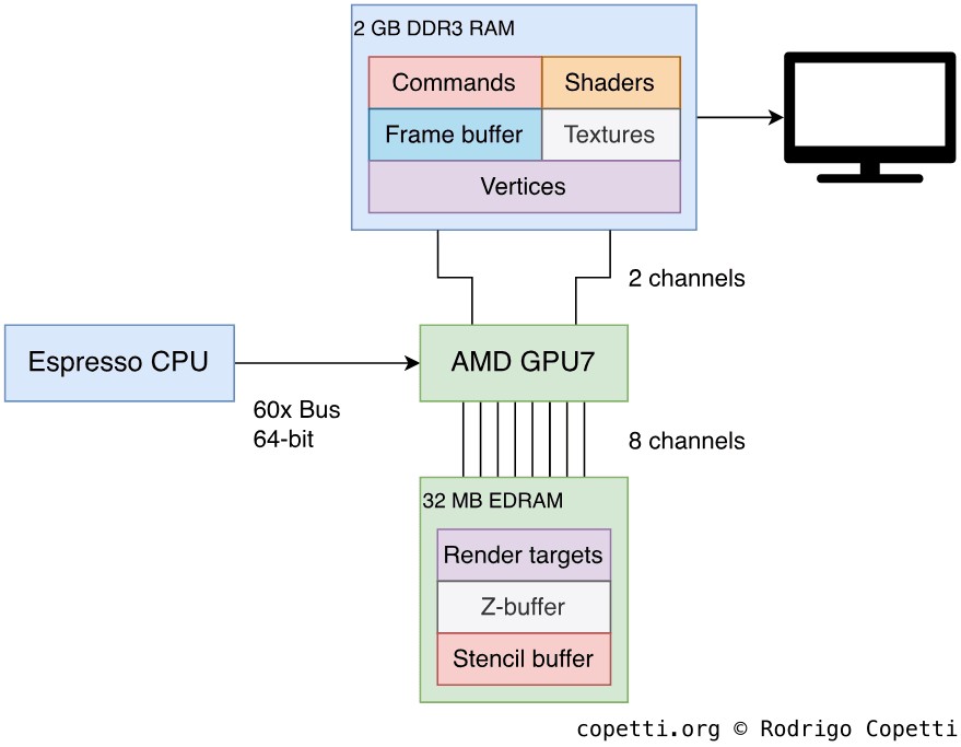
Example of how data is organised across the memory available.
Conversely, the Wii U's EDRAM is larger than the Xbox 360's (meaning the need for tiling is reduced). However, it does not include dedicated circuitry for post-processing.
Constructing the frame
This is the signature section of the Architecture of Consoles series where I attempt to explain the process of converting the geometry (coming from the CPU) into pixels (which users eventually see on the telly). Nevertheless, in this article, the explanations will be a bit different as the fundamentals of TeraScale were already explained in the Xbox 360 article.
The most important changes since Xenos is the implementation (or better said, standardisation) of Geometry Shaders and Compute Shaders, both of which take advantage of the new capabilities of the unified shaders. This doesn't mean GPU7 had to be completely redesigned to make way for these two stages, what happened is that APIs had been expanded to enable new applications without considerably changing the existing circuitry.
Being an AMD/ATI chip built for a Nintendo console, GX2 supports two shader APIs, OpenGL's GLSL 3.3 and OpenGL ESSL. The SDK also comes with some extensions to provide functionality only available on GPU7, but it doesn't support OpenCL and certainly not Direct3D.
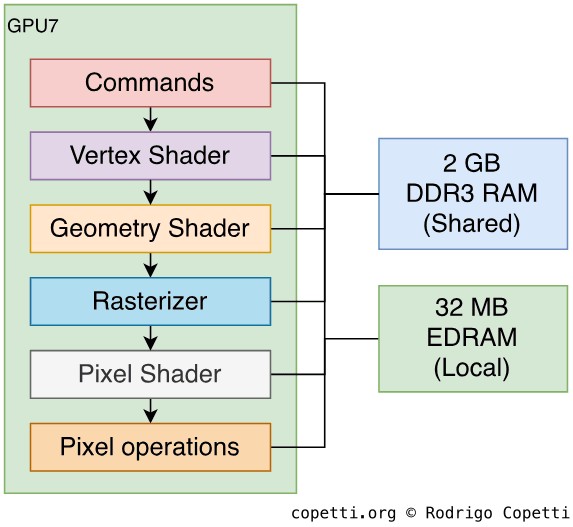
Overview of the graphics pipeline in GPU7.
Be as it may, GPU7 still inherits the designs of the Radeon R700 series, so GPU7's pipeline is somewhat aligned to Direct3D 10.1 and OpenGL 3.3 standards. Although, their respective shader languages aren't natively understood by GPU7 (they require proprietary compilers shipped with the official SDK).
As a side note, typical Radeon cards for the PC market use AGP or PCI-e bus interfaces. Well, the Wii U hardware still relies on the old-school practice of exposing I/O registers as memory locations . I guess neither Nintendo nor AMD were concerned as this is all part of a custom design.
Let's now go over the pipeline, stage by stage. Since the design is very similar to the Xbox 360's Xenos GPU, I'll try to focus on the novelties of GPU7 instead to avoid repeating information.
Commands
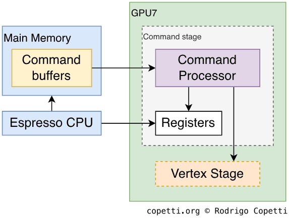
Overview of the command stage.
With most graphics cards, especially ATI/AMD ones, the starting point is always the Command Processor . As we've seen many times before, this is the door between the GPU and the outside world (i.e. the CPU).
In the case of the GPU7, the Command Processor reads commands stored in RAM and activates the necessary engines within the chip. Most notably, GPU7 features a dedicated Direct Memory Access (DMA) controller to manipulate data between MEM1 and MEM2 without the intervention of the CPU.
Furthermore, DMA may work asynchronously (out of pace with the rest of the circuitry), so GPU7 provides a few commands to refresh its cache and synchronise with DMA (in the form of a semaphore) to maintain order.
Vertex
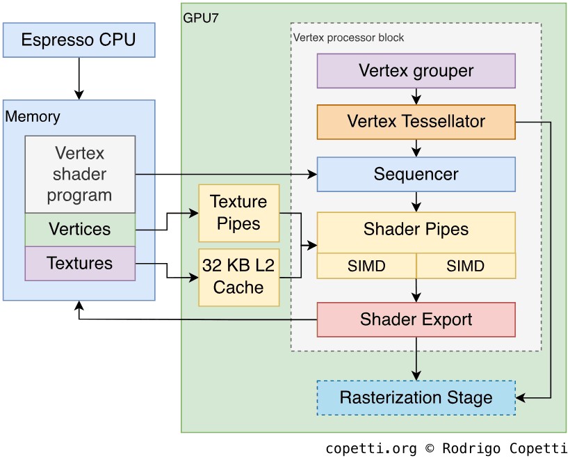
Overview of the vertex stage. You'll soon find that this stage and the pixel stage are not that different.
At first glance, this stage is pretty much in line with Xenos/Crayola except that some blocks have been expanded (increased cache) while others have contracted (reduced number of ALU units and the Memory Export path is shorter). None of this necessarily means a performance decrease, however, as let's not forget GPU7 is ~7 years ahead of Xenos.
To start with, let's take a look at the ALUs. Xenos resorted to three shader pipes (blocks of 16 ALUs) to execute the vertex shaders. GPU7 only bundles two blocks of 16 ALUs, but each block is now wrapped around a larger circuitry named SIMD processor, which I assume denotes the addition of larger circuitry (dedicated 8 KB of L1 cache, plus the extra interfaces and control units) to sustain more concurrent traffic. Furthermore, each ALU is made of four 'sub-ALUs', allowing the former to compute vectors made of four scalars at once. ATI/AMD calls these sub-ALUs stream processors and it's a common marketing term.
Now, instead of the Sequencer dispatching the calculations right away as they come, they are first combined into a larger batch of 64 vertices along with some meta-data to control the operation , this is called a Wavefront. The batch is then sent to the two SIMDs and, considering the fact there're only 32 ALUs in GPU7, they take four cycles to be computed.
I assume this new design is what enables manufacturers to devise different ranges of graphics cards, with the most expensive including more SIMD units (thus taking fewer clock cycles to complete). As game consoles are not particularly famous for embedding high-end hardware (instead, they compensate by being more efficient), four clock cycles are what it takes in the Wii U to process a Wavefront.
Geometry
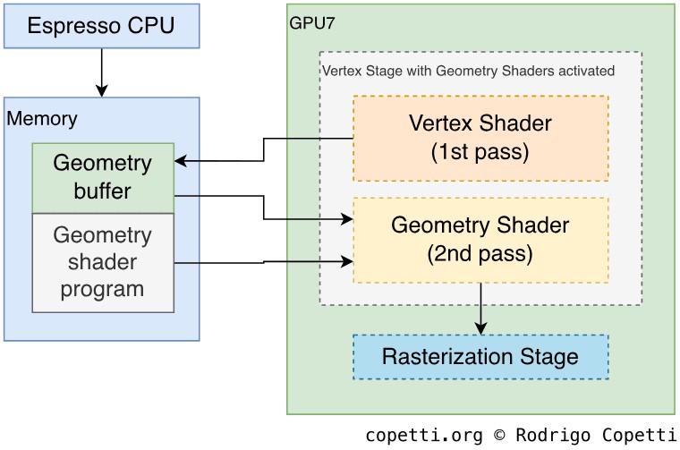
Overview of the geometry stage.
The geometry shader is a new stage of the graphics pipeline that appeared right after the two famous APIs (Direct3D and OpenGL) incorporated the unified shader into their specification. The purpose of this new stage is to allow developers to manipulate primitives (points, lines or triangles) as opposed to single vertices . This can be useful for procedurally generating new geometry out of existing one (i.e. devise shadows, fur and so forth). The GPU7, like the Radeon R700, inherits compliance with OpenGL 3.3 and therefore supports this new shader type.
Behind the scenes, however, the geometry stage is just another 'mode' of the vertex stage. To make a long story short, if geometry shaders are activated, the vertex stage doesn't forward the data for rasterisation right away. Instead, the outputted data is saved into a dedicated buffer in MEM2 and the vertex stage starts over but fetches data from the geometry buffer. Then, Wavefronts are assembled to grab the indices of up to 64 primitives along with meta-data denoting a geometry shader will be executed. Afterwards, the Sequencer reads the new Wavefront, parses the primitives and sends them to the two SIMDs for computing. The process is repeated until all primitives are processed.
Finally, the pipeline continues to the rasterisation stage.
Rasteriser
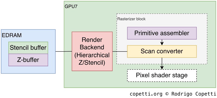
Overview of the rasteriser stage.
The rasterisation stage tends to be much simpler than other stages. The main reason being the act of converting vertices into pixels is mostly systematic, and no extra programmability is needed (aside from a few parameters available to tweak). As such, this stage is identical to Crayola/Xenos.
Be as it may, the Z and stencil buffers are not allocated on dedicated memory anymore. Instead, the new Render backend block (performing Z and stencil testing, with support for hierarchical testing as well) must access RAM to work (either EDRAM or main RAM).
The rasteriser can compose frames of up to 8192 x 8192 pixels using 128-bit pixel formats . This would allow massive frames with HDR colour quality. However and for obvious reasons, developers don't need frames that big (1280 x 720 will suffice for this console), except HDR which will be used thoroughly.
Fragment
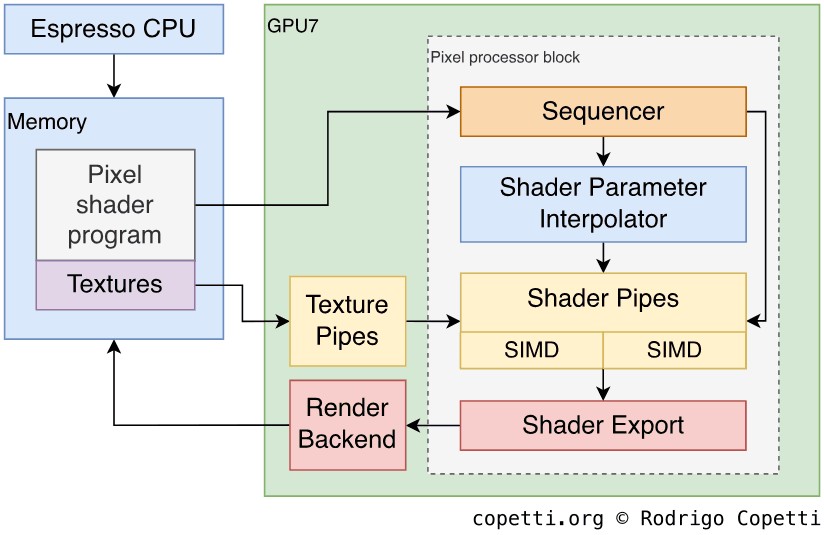
Overview of the Pixel/Fragment Shader stage.
The pixel shader stage follows the same methodology as the vertex shader except it's now pixels being shuffled around. After going through Xenos' pixel capabilities and GPU7's new vertex pipeline, I'm afraid there's not a lot left to explain here.
The block that fetches textures to the SIMD units is now called Texture Pipe and there're two of them. Each contains 8 KB of L1 cache and they both share 32 KB of L2 cache when accessing RAM. Additionally, they can perform up to 16x Anisotropic filtering on the spot and can also fetch cube maps (used for environmental mapping/reflections).
I guess it's worth pointing out that the shader model (OpenGL GLSL 3.3) adds an abundance of new routines (i.e. new types of texture blending, bitwise operators, texture swizzling) for manipulating textures and removes many constraints (such as the number of instructions allowed per shader). All of which makes the life of developers a bit easier.
Pixel Operations
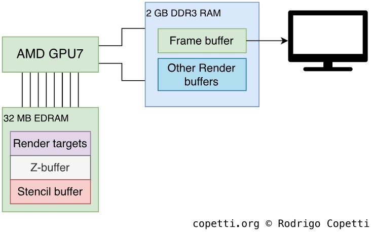
Overview of pixel operations available.
Once the frame has been rendered, developers can apply more Z-testing (in case it wasn't activated at an earlier stage), colour blending and, finally, export the pixels to the frame-buffer for display. This is all performed by the Render backends (there's of two of them) which are found at the end of the Pixel shader stage.
Finally, even though the Wii U doesn't feature the sophisticated circuitry that the Xbox 360 bundles within its EDRAM module, there are still many interesting capabilities provided by GPU7. This includes automatic Multisample Anti-aliasing of up to 16 passes (MSAA 16x) to soften edges, which surprisingly doesn't require tiled rendering since the larger 32 MB of EDRAM (MEM1) of the Wii U is more than enough for these operations (well, maybe MSAA 16x will eat up too much MEM1, however, MSAA 8x is still acceptable).
Apart from that, we have to take into account the custom algorithms programmers may decide to implement. This is thanks to the flexibility of the APIs and the vast amount of shader operations available, including Compute Shaders (which offload CPU computations into the GPU).
Interactive comparison
I've added new 3D models on the interactive viewer so you can check out the before (Hollywood's GPU) and after (Latte's GPU/GPU7) 'effect' by yourself:


Interactive model available in the modern edition
Super Mario Galaxy (2007) for the Wii.
4,877 triangles.


Interactive model available in the modern edition
Super Mario 3D World (2013) for the Wii U.
9,304 triangles.
While Mario's textures don't seem to offer a lot of extras on the Wii U, GPU7's improvements lie in the extra surfaces and bones, especially on the hands and face, which make the model react more realistically to ambient effects and animations. In doing so, scenes look more natural throughout gameplay.
Video decoding
An additional feature beyond the 3D rendering capabilities of GPU7 is the inclusion of H.264 decoding circuitry that transforms streams of H.264-compressed data into raw frames that the GPU can understand (and subsequently render on the screen). The main advantage being bandwidth efficiency without performance penalties.
Consequently, the H.264 block is used for displaying motion video on the game in any way the developer prefers (i.e. within gameplay or as a cinematic).
Video Output
Time has come for Nintendo to ditch their proprietary analogue circuitry and embrace (at least one!) video standard. Lo and behold, an HDMI 1.4 socket is finally included on the back, along with the traditional AV Multi Out as a 'backup'.

Back view of the console, showing both video options (HDMI and Multi AV).
Now, even though the output resolution can go as high as 1080p, most games resort to 720p to balance game performance with the use of anti-aliasing and a large resolution. Using 720p also helps developers to keep support for 480i and 576i without altering the game logic (as the video encoder takes care of automatically downscaling the frame). This modus operandi matches the one of the PlayStation 3 and the Xbox 360.
A secondary GPU
With all being said, how come this console can still play Wii games? Is there some sort of GPU7-to-Hollywood emulator running behind the scenes? Well, the short answer is no. It may surprise you Nintendo went straight ahead and added the old GPU circuit from Hollywood (let's call it 'Wii GPU') inside Latte as well . This block only works when a Wii game is running. Although, the Wii GPU houses the old 3 MB of 1T-SRAM which is the one we now know as MEM0. So, at least the extra memory is used by the new hardware.
Furthermore, Nintendo also fitted an extra chip called DMCU to replicate the old Video Interface. According to fail0verflow, the DMCU is just a Motorola 68HC11 controller programmed to behave like the precursor. Its only purpose is to receive commands from Wii games and forward the frame to GPU7, so the latter can broadcast it to the TV. Due to the fact Wii games are made for PAL/NTSC screens, the GPU7's video encoder must upscale it (which, in my experience, is not very good at doing so...).
If you wonder, there's no 'Wii GPU and GPU7' co-processing available for Wii U games. It would've been 'interesting' though, albeit knowing one would bottleneck the other...