Alrighty, back to the digital architecture, let's see now how games construct the frames and music you see and hear.
For the CPU, Nintendo employed a customised version of the NEC V810, operating at an impressive 20 MHz (considering the SNES averaged at 1.79 MHz and the GameBoy ran at 4.19 MHz, imagine what this one's capable of!). The company refers to it as NVC because the chip shipped with the Virtual Boy combines a V810 core with several additional components, which we'll examine in the next paragraphs.
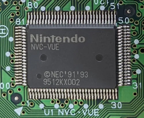
The NVC chip.
To start with, the V810 is part of the V800 CPU family that NEC designed for the embedded market . While this CPU wasn't as popular as the competition (such as the MIPS series or the Motorola 68000) it does offer a range of cutting-edge functionality, specifically:
- The V800 series Instruction Set Architecture (ISA): A RISC instruction set that mixes 16-bit and 32-bit instructions.
- Thirty-two 32-bit registers: The V810 is a complete 32-bit CPU and the registers are well aligned to that architecture.
- As common with RISC CPUs,
r0is always zero.
- As common with RISC CPUs,
- A 32-bit address bus: Enabling to access up to 4 GB of memory, an enormous amount for its time.
- A five-stage pipeline: See a previous article for a detailed explanation of instruction pipelining. Notably, while other systems debuted with three pipeline stages, this one went straight for the five.
- To avoid hazards, NEC resorted to hardware interlocks to stall the pipeline automatically.
- 1 KB of L1 Cache for instructions.
- Interestingly, you won't see another 'cached' handheld from Nintendo until the Nintendo DS arrives nearly a decade later!
This was exceptionally sophisticated for a portable console in 1995, but Nintendo went even further by incorporating additional resources:
- I/O interfaces: These handle the communication with proprietary accessories.
- 16-bit external bus: The V810 can be configured with either a 16-bit or 32-bit bus. Well, Nintendo's engineers opted for the former.
- This introduces some penalties (i.e. wait states) with 32-bit memory transfers, but as you'll soon see, programs weren't that demanding.
- A timer: This is just a 16-bit counter.
- A wait control: Stalls the CPU depending on the external bus accessed. This is because the V810 treats all memory as uniform. In practice, accessing the Game ROM is slower than, let's say, internal RAM. So, this component corrects the timings accordingly.
While all of this seems fine and dandy, it does come at a big cost: six AA batteries. This likely explains why companies clung to older technologies in portable devices, at least throughout the 90s.
Memory access
32-bit addresses look very tempting on paper, but if the system won't utilise anything close to 4 GB of memory locations, then it's a huge waste of resources. For instance, even though the upper address lines remain unchanged, they are still decoded during every memory read.
So, for good reasons, Nintendo cut down to 27-bit addressing. This means that up to 128 MB of memory can be accessed instead. The system still uses 32-bit words for addresses, but the upper 5 bits are discarded. As a result, some regions of the memory map are mirrored.
Having said that, the memory map layout enables the CPU to access the majority of the components that make up this system. This includes :
- 64 KB of RAM for general-purpose use. For that reason, Nintendo calls it 'Work RAM' or 'WRAM'.
- The type of chip fitted is called PSRAM (short for 'Pseudo-Static RAM' or 'Pseudo-SRAM'), which incorporates self-refreshing Dynamic RAM (DRAM). This setup is both faster and more energy-efficient than the traditional low-cost DRAM.
- The cartridge ROM and any onboard RAM (if present).
- The sound chip.
- The graphics chip, along with its dedicated memory.
- I/O interfaces and their respective registers.
This is as far as the CPU goes, now it's time to see what you can do with it!