Similarly to Nintendo, Sony built an extremely packed System-on-Chip (SoC) that houses most of the components we are going to discuss throughout this article. This includes the main CPU in charge of executing games and other programs (unlike the other CPUs, which we'll talk about in due time). The SoC is called Tachyon, a name chosen by Sony themselves.

The Tachyon chip on the original PSP model.
The main CPU is an in-house design that keeps up with the tradition of using MIPS technology. Be that as it may, it's been four years since the release of the PlayStation 2, I wonder what's the state of MIPS since then?
MIPS after the turn of the century
I'm afraid the golden years of MIPS were left in the 90s, and there aren't any indicators that these will repeat anytime soon. Its parent company, SGI, lost dominance against affordable x86 workstations and was running out of cash. So, in 1999, it sold its majority stake in MIPS . With this, MIPS became an independent company once again; however, the competition was fiercer than in the early days.
The company's first decision was to acknowledge that MIPS CPUs couldn't compute in the high-performance arena anymore. So, they shifted their focus to low-power computing, running head-to-head against ARM and its unprecedented popularity.
Consequently, MIPS revisited its fragmented CPU line and consolidated it with three instruction sets :
- MIPS32: An update of MIPS II - the last 32-bit-only Instruction Set Architecture (ISA) - bringing functionality gathered from later architectures while keeping the 32-bit boundary.
- MIPS64: The continuation of MIPS V, a 64-bit ISA and the last one before the revamp. The MIPS V was a superset of all previous ISAs, just like its predecessors.
- microMIPS: Available as 'microMIPS32' and 'microMIPS64', these are supersets of the MIPS32 and MIPS64, respectively, with an additional group of 16-bit instructions (à la Thumb). microMIPS is not binary compatible with the other ISAs, however, so it required re-compilation of legacy codebases to run on microMIPS.
The big difference was that these would now be developed in conjunction, as opposed to MIPS dropping the previous architecture as soon as the next one arrived. New revisions would be denoted with the 'Release x' suffix, such as 'MIPS32 Release 6' or 'MIPS32R6', which is the last revision to date.
Along with the ISAs, MIPS also started selling a new line of IP cores. For instance, the MIPS32 4k design implemented the MIPS32 R2 ISA; it came in different variants and offered plenty of customisations.
Back on topic, Sony presumably acquired a license of the MIPS32 4k and customised it by extending the ISA and bundling particular co-processors . The result is called Allegrex and runs at a variable speed, from 33 MHz to 333 MHz.
The new portable CPU
Allegrex is a complete 32-bit core offering :
- A custom MIPS ISA: mixes MIPS32R2 instructions with exclusive ones for arithmetic operations (multiplication, subtraction, min/max, bit-shifts) and interrupt control. These are called 'Allegrex Extended Instructions'.
- A 32-bit address bus: this means that up to 4 GB of memory can be seen by this CPU.
- 32 general-purpose registers: all of them store 32-bit values; and two (the zero register and link register) are reserved for special uses. By now, this should come as no surprise.
- A 7-stage pipeline: one more stage than its home sibling.
- 32 KB of L1 Cache: of which 16 KB is for instructions and 16 KB for data.
- A cache write-back buffer: the CPU can write over the cache and assume RAM has been updated as well. Meanwhile, the cache takes care of updating memory as soon as its internal buffer is full.
- This design speeds up memory stores, but doesn't work right away with multi-processor systems like this console . So, developers had to manually evict the buffer when other components depended on the new values in memory.
Overall, this looks more competitive than the ARM9-based competition, but it's not over yet, as we still need to check the co-processors cooperating next to the core.
Coprocessors
As with any MIPS CPU, Allegrex has three coprocessor slots. Sony added three :
- The System Control Coprocessor as 'CP0': a necessary building block of any MIPS CPU. This particular component is what enables memory protection, cache coherency and interrupt control in the core itself .
- A Floating-Point Unit (FPU) as 'CP1': accelerates arithmetic operations with 32-bit decimal numbers (following the IEEE 754 standard). It has thirty-two 32-bit registers and an independent 8-stage pipeline, thereby adding more parallelism to the main CPU.
- A Vector Floating-Point Unit (VFPU) as 'CP2': a coprocessor designed for vector operations, similar to a traditional SIMD processor. Compared to the FPU, it instead provides 128 32-bit registers, relies on a proprietary instruction set, and implements a variable-length pipeline. The VFPU operates up to 32-bit floating-point values, which can be grouped into a 4-component vector or even a 4x4 matrix. This is useful for computing different kinds of geometric operations without requiring to rearrange the data.
- Its efficiency comes from its 128-bit data bus connected to the rest of the system, offloading the main CPU's transit.
- Unlike the FPU, some behaviour of the VFPU deviates from the IEEE-754 standard.
In conclusion, Allegrex is incredibly fast. However, we still don't know what you can do with it. After all, you can imagine this CPU as the conductor of an orchestra, and we haven't checked out the performers yet.
A focused memory management
Let me talk for a moment about the memory system implemented in this system. Among other things, the System Control Coprocessor provides the functionality of a Memory Protection Unit or 'MPU' (not to be confused with an 'MMU'), which maps the physical hardware onto the CPU's memory space with some special quirks in between. Even though its modus operandi can be seen as a bit primitive at first, we'll see why it's optimal for the needs of this console.
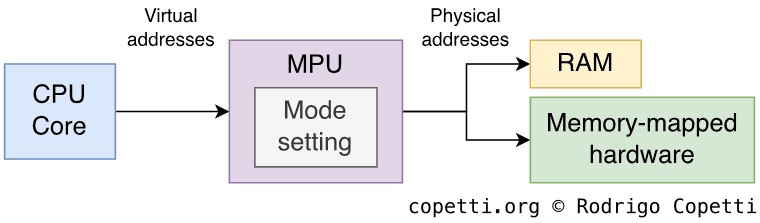
Memory addressing with the MPU.
A traditional Memory Management Unit or 'MMU' takes care of the CPU's access to the components surrounding it. This implies that all the address lines of the CPU will be connected to the MMU; only the latter is connected to the rest of the system.
This is particularly advantageous for features like 'virtual memory' and 'memory protection'. Well, to achieve virtual memory, an MMU must bundle a component called 'Translation Lookaside Buffer' (TLB) to prevent performance degradation. Now, Allegrex's MMU lacks a TLB , so it focuses on memory protection. This is why Allegrex's MMU is instead called an MPU (Memory Protection Unit). An MPU is a cut-down version of an MMU without virtual memory. In any case, memory protection gives the system the power to decide which memory locations a program can access.
Thanks to this, Allegrex won't have to deal with userland programs (e.g. games) accessing restricted locations (e.g. encryption keys). To enforce this restriction, memory addresses are grouped into five segments with different privilege levels. Furthermore, Allegrex's MPU contains three modes of operation: User mode, Supervisor mode and Kernel mode.
If a casual process (operating in user mode) wants to access a memory address found in a privileged location, the MPU will ask the operating system (through the use of 'exceptions') whether to grant permission to this process.
All in all, this allows Sony, the developer of the operating system, to implement a security system enforced by hardware.
Memory available
So far, we've analysed the PSP's main CPU and its accelerators. Now let's see the physical memory available in this system.
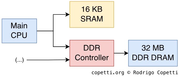
Memory layout from the main CPU perspective.
The PSP comes with two memory blocks accessible from the CPU :
- 16 KB of SRAM: this is what we called Scratchpad in previous articles. It's small but very fast RAM, so it's up to developers to make proper use of it, although unofficial documents have called it 'useless' .
- 32 MB of DDR SDRAM: a significantly larger amount at a lower access rate. We'll refer to it as 'main memory' across the article.
- The 'DDR' initials mean 'Double Data Rate', which denotes an evolution from the traditional 'SDRAM', now featuring a faster transfer protocol. The original Xbox used the same type.
Bus design
You'll soon find that the PSP accommodates lots of components with unique functionality. So, to organise them without repeating previous mistakes, Sony's engineers interconnected them using dedicated buses. Thus, only small groups of components, with similar applications, share the same bus. Those buses talk to each other using dedicated arbiters (in the form of 'memory controllers' or Direct Memory Access (DMA)).
All of the buses found in Tachyon implement a well-known design called Advanced High-performance Bus (AHB), a solution built by ARM to tackle congestion on their chips and SoCs. If you are curious, AHB was also adopted on the Wii.
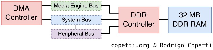
Basic layout of the three main buses in this system.
Using the principles above, the following buses were constructed for the PSP :
- The System Bus: connects the CPU, scratchpad and GPU. It's 128 bits wide.
- The Media Engine bus: connects another group of components (explained in the next section). It has the same properties as the System Bus.
- The Peripheral Bus: connects I/O and storage-related components. It's 32 bits wide.
All three buses connect to the DDR controller, which is where the main RAM is found.
Tackling traffic congestion
Inside each bus, there will be multiple components working independently. They will store processed data in a shared space (such as the main RAM). Now, we don't want the CPU to intervene whenever a module needs to read or write from memory. Traditionally, a DMA unit was placed on the bus to provide this facility, but a single DMA can only do so much. The PSP contains a significant number of components, and this will eventually lead to bottlenecks.
The solution is very simple: bus mastering. In a nutshell, each component will get its own DMA controller. This gives them the ability to become the 'bus master' and take control of the bus to access whatever location they want. To avoid contention (multiple 'bus masters' at the same time), the neighbouring components will acknowledge this event and wait until the operation completes.
The end of the line
The RISC revolution produced countless CPU designs throughout the 80s and 90s, but only a handful endured beyond the turn of the century. Just like I concluded my analysis of the SuperH in the Dreamcast article, the PlayStation Portable will be my last article of this series to feature a MIPS CPU.
After many turnarounds, what's left of MIPS is now a company designing RISC-V CPUs. In all fairness, this is an interesting strategy that provides the company with greater leverage to compete against ARM.
Looking back at my analyses, however, it's hard to comprehend how such a talented company could have lost its market share. Admittedly, in the workstation market, it became clear that Intel's x86, no matter the amount of criticism, won by making equipment affordable (thanks to its Pentium line, along with the 'clones') and attractive due to its (Windows-only) compatible software. Finally, the P6 architecture provided Intel with the scalability initially only enjoyed by RISC designs.
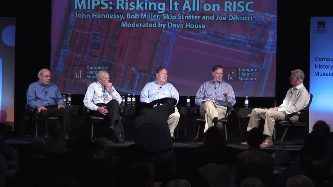
In 2011, the Computer History Museum (Mountain View, California) conducted an interesting interview with MIPS co-founders and former executives , where they talked about MIPS' beginnings, its impact on the industry, and eventual reorganisation.
In the case of low-power computing, it was harder for me to understand the retreat, as MIPS and ARM shared similar business models based on IP licensing. Luckily, a previous interview conducted by the Computer History Museum in 2011 raised the same question, resulting in this answer:
We made a mistake, we didn't realise how important the cellphone market was. Early there was no money to be made (...) but ARM got it by investing in it. It was a very smart move and it turned out to be an incredible leverage point. We just looked at the gross margin and said "that's not a great return! we'd be better off putting our attention elsewhere" but of course, it turned out cell phones became smartphones [and then] became a gigantic.
- John Hennessy, co-founder of MIPS Computer Systems
Nevertheless, when it comes to this topic, I believe that, while we are unlikely to see a new MIPS CPU, we will see its former engineers carry MIPS' distinctive technologies into new projects.
That being said, let's continue with the PSP analysis.