At the heart of this console, we find a powerful package called Emotion Engine (EE), a joint project by Toshiba and Sony running at ~294.91 MHz .
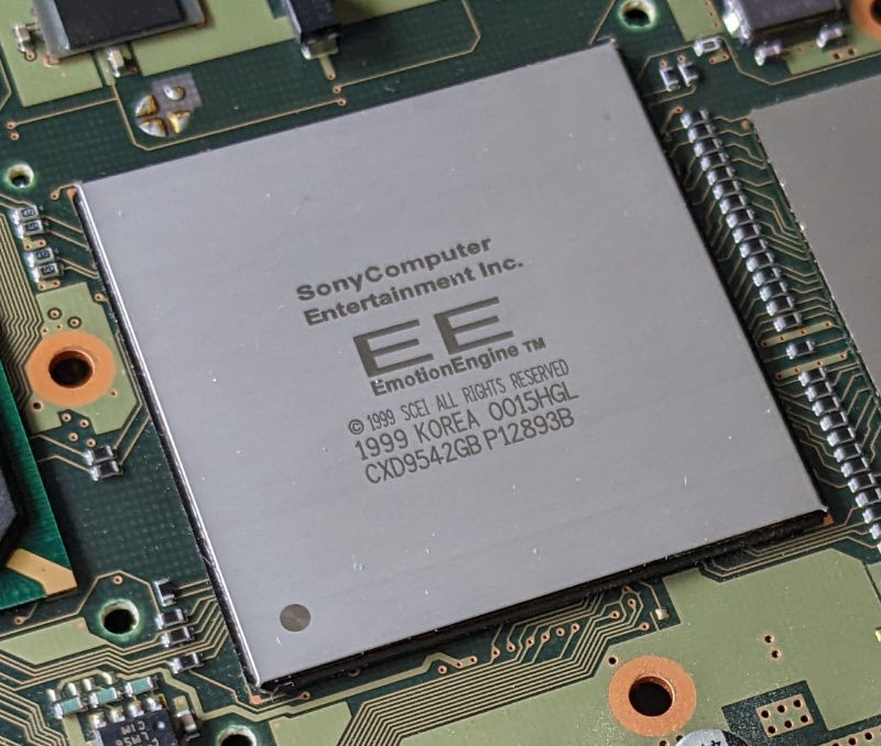
The Emotion Engine, as seen on the first motherboard revision of this console.
This chipset contains numerous components, one of them being the main CPU. The rest are at the CPU's disposal to speed up certain tasks. For this analysis, we'll divide the EE into three sections:
- The leader: The main component that controls the entire chip.
- The memory available, a crucial ingredient that enables the processors to do meaningful operations.
- The co-processors: These accelerate particular computations.
The leader
In a nutshell, the main CPU is a MIPS R5900, an exclusive MIPS core designed for this console. You may recall how Sony started venturing into MIPS silicon with the very first PlayStation (where we can find a MIPS R3000A second-sourced from LSI). For the next generation, we've got a MIPS 'R5900'... but what does that name mean for us?
To understand what's hidden behind these new numbers, let's take a look at some history surrounding that era.
Outperforming success
The MIPS R4000 was a popular CPU series adopted by a wide range of systems, including a close competitor. Thanks to its success, MIPS brought a once-unaffordable range of advancements (64-bit computing, 8-stage pipelines, and so forth) to the masses.
Fast forward, the next big leap arrived in 1995, with the release of the R10000. Now under the funding of SGI, MIPS produced a new processor that took the R4000's parallelism capabilities miles further, debuting techniques like :
- Speculative execution: The CPU predicts the result of conditional branches before they are computed. These predictions are based on previous results stored in an internal 512-entry table. Once the condition is computed, if the prediction turns out to be correct, the CPU has saved valuable time. Otherwise, the extra computations are discarded.
- Thanks to this, MIPS finally turned a recurring problem (control hazards) into an advantage.
- In other CPUs, you may find similar functionality referred to as dynamic branch prediction.
- 4-issue superscalar pipeline: Building on the pipelined design, the CPU could now fetch up to four instructions at the start of the pipeline, and distribute them across separate units, allowing the CPU to execute these instructions at the same time. In doing so, the CPU achieved a greater degree of parallelism.
- Out-of-order execution: The CPU could also re-arrange the sequence of instructions to keep its units as busy as possible... as long as doing so didn't introduce any hazards.
- L2 cache with a 128-bit bus, enabling to pull more data into the CPU at a time, which was becoming a necessity given the previous enhancements.
Such innovation came at the cost of a complex design, however, and the final product was anything but cheap. SGI only bundled it with high-end equipment, and any attempt to bring it to a home console was out of the question.
High-end for the masses
Even before it reached the market, MIPS was already aware of the commercial limitations of the R10000. So, they hired Quantum Effect Devices (QED) to develop an affordable version of the R10000 for the mid- to low-end market.
As a company founded by former MIPS employees, QED was in the business of designing variants of MIPS cores for the budget sector. They had previously engineered the R4600 Orion, a cut-back version of the R4000, in a similar fashion to the VR4300 (found in the Nintendo 64). Orion was also tailored for Windows NT workstations .
In the end, QED came back with a new core called the R5000. It was a continuation of Orion, but was marketed as a cheaper alternative to the R10000, with significant cutbacks :
- In-order execution.
- No speculative execution.
- Superscalar capabilities limited to two instructions (2-issue), with no parallel integer instructions. However, floating-point instructions can still be paired with others.
- As a consequence of the previous choice, L2 cache uses a 64-bit bus instead.
Consequently, this became an ideal CPU for powering modest equipment, such as SGI's low-end workstations. In any case, notice that the cut-down pipeline could still perform concurrent floating-point operations, as if QED had planned to keep the CPU as an attractive product for vector/3D applications. You'll soon see that another company quickly took note of that, as well.
As a side note, it's curious to observe that, on the other side of the pond, there were similar advancements in the opposite direction: ARM joined forces with DEC in the pursuit of lifting ARM chips into the high-end market.
Now that we've seen the state of the industry, let's turn to Sony's partners.
A special order for Sony
Toshiba had been a MIPS and QED licensee for some time , and was no stranger to commercialising MIPS packages. The company was also manufacturing their own MIPS-compatible core, called TX39 , derived from the MIPS R3000 . At one point, Sony and Toshiba joined forces to produce a CPU exclusively tailored to Sony's upcoming console.
This was a tremendous benefit for Toshiba: very often CPUs are required to fulfil a wide range of requirements from different stakeholders, and in doing so it constrains opportunities for specialisation. Now, there was only a single purpose: 3D gaming. Thus, leaving plenty of room for all kinds of innovation.
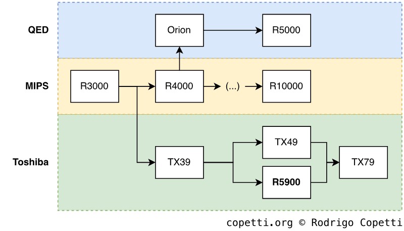
CPU lineage leading to the R5900.
That being said, Toshiba ended up grabbing their TX39 design and combining it with ideas from their upcoming TX49 core, the R5000, and vector accelerators. The new core was called R5900 and introduced the following '3D' enhancements :
- A variation of the MIPS III ISA. This includes the original 64-bit ISA previously seen on the Nintendo 64, but extended with interesting opcodes. Sony added some instructions from MIPS IV (prefetch and conditional move), along with their own SIMD extension - called multimedia instructions - to accelerate vector calculations (similar to the SH-4, but integer-only).
- The multimedia instructions are still 32 bits wide, but can operate up to three 128-bit vectors at a time. They offer operations such as vector arithmetic, min/max, and many kinds of scalar combinations for forming new vectors.
- 32 128-bit general-purpose registers: Another significant Toshiba-branded enhancement. Forget about the typical 32-bit storage; we've stepped into the 128-bit realm now. Nevertheless, the majority of operations will hardly use all the available space (MIPS words are still 64-bit long). This is where the aforementioned multimedia extension comes into play, as its instruction set makes full utilisation of the extended register file.
- When using the new instructions, each register can store vectors made up of many types of scalars (from two 64-bit integers to sixteen 8-bit ones).
- To prevent performance penalties, these registers are accessed through a 128-bit bus, while the rest of the CPU uses an internal 64-bit data bus.
- Two 64-bit ALUs. Each can operate on 64-bit integers independently, but they can also be combined to form a 128-bit ALU. The latter is the brain behind those shiny multimedia opcodes.
Aside from these, we also find other improvements that developers may welcome as well:
- A 6-stage pipeline: That's one additional stage compared with the predecessor's.
- 2-way superscalar execution: Thanks to the two ALUs, up to two 64-bit integer operations are now executed in parallel.
- This restores another advantage of the MIPS R10000.
- 24 KB L1 cache: Divided into 16 KB for instructions and 8 KB for data.
- The circuitry also implements a prefetch function to cache instructions and data before they are requested. This is done by including extra logic that can identify which places in memory are requested more often.
- 16 KB of Scratchpad RAM, also known as 'Fast RAM'.
- Memory Management Unit (MMU): Interfaces memory access with the rest of the system.
Moreover, the core is complemented by a dedicated Floating-Point Unit (FPU) - identified as 'COP1' - that accelerates operations with 32-bit floating-point numbers (also known as floats in C). This is a peculiar block, as it doesn't follow the IEEE 754 standard, most notably because it lacks support for infinity (which is computed as 0 instead) . Apart from that, it features 32 32-bit registers.
A recognisable memory choice
Next to the Emotion Engine are two blocks of 16 MB of RAM, giving a total of 32 MB of main memory. The type of memory used is Rambus DRAM or 'RDRAM' (déjà vu!), which is accessed through a 16-bit bus.
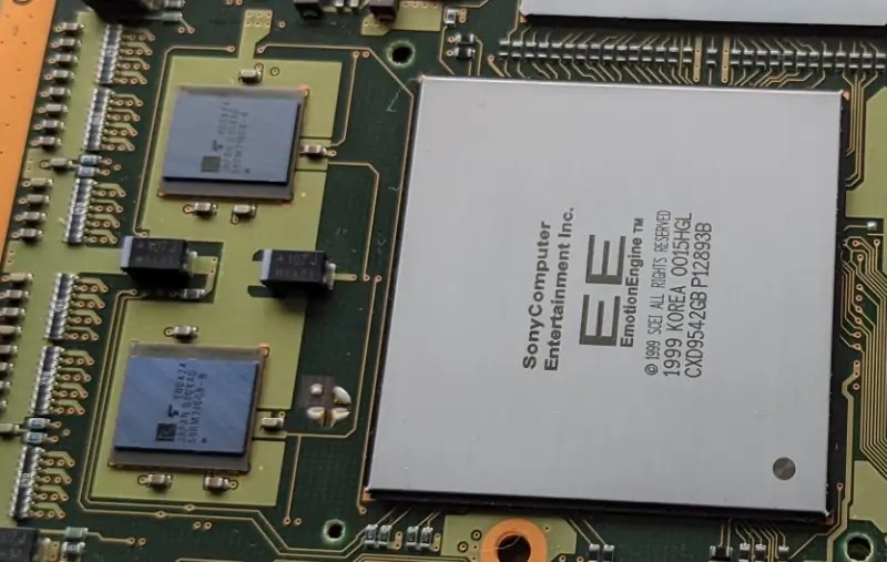
The two RDRAM chips next to the Emotion Engine.
At first, this can be a little disappointing to hear, considering the internal bus of the Emotion Engine is as wide as 128 bits. However, the RAM chips are strategically arranged using a dual-channel architecture, where both chips are connected through two independent 16-bit buses (one bus per chip) to improve data throughput. The resulting setup provides a theoretical 3.2 GB/sec, so rest assured that memory latency is not an issue in this console!

Memory design of the Emotion Engine. You can guess where the congestion will emerge.
At one corner of the Emotion Engine, there is a powerful Direct Memory Access Controller (DMAC) that transfers data between main memory and Scratchpad, or between main memory and any component inside the EE.
Data transfers are carried out in batches of 128 bits, but here is the interesting part: every eight batches, the main bus is temporarily unlocked. This leaves a small window in which to perform other DMA transfers in parallel (up to ten), or to let the CPU use the main bus. This modus operandi is called slice mode, and is one of the many modes available on this DMA unit. Bear in mind that, while slice mode reduces stalls on the main bus, it does so at the cost of slowing down the overall DMA transfer.
Preventing past mishaps
Whether we want it or not, with the amount of traffic flowing through the Emotion Engine, this design will eventually suffer the consequences of the Unified Memory Architecture or 'UMA'. That is, multiple independent components trying to access main memory at the same time, causing congestion. Well, to tackle these issues, Sony alleviated the constant demand for memory by:
- Wrapping their processors with lots of cache, thus requiring access to main memory only when absolutely necessary.
- 99% of cache/Scratchpad mentions in this article will be for this reason.
- Adding a 128-byte Write Back Buffer: Very similar to the Write Gather Pipe, but instead of waiting until it's 25% full, it checks the state of the bus (i.e. congested or free) first.
This sounds very convenient for applications that can benefit from cache, but what about those tasks, such as manipulating Display Lists, which shouldn't consume cache at all? Luckily, the CPU provides a different memory access mode called UnCached, which only uses the Write Back Buffer. As a result, it won't waste cycles correcting the cache (product of cache misses).
Furthermore, the UnCached accelerated mode is also available. This one adds a buffer for speeding up the reading of adjacent addresses in memory.
Other interesting bits
Inside the same Emotion Engine package, there is yet another processor called Image Processing Unit or 'IPU', this time designed for image decompression. As the successor to the MDEC, the IPU can be useful when a game needs to decode an MPEG2 movie without jamming the main CPU.
Long story short, the game sends compressed image streams to the IPU (hopefully using DMA), which then decodes them into a format that the GPU can display. The PS2's operating system also relies on the IPU for DVD playback.
Finally, the IPU can also process compressed high-resolution textures, reducing CPU usage and the amount of data that needs to be transferred.