This section tends to be very rich in technologies considering Nintendo's consoles favour generous I/O before state-of-the-art CPUs and GPUs. Let's see what the Nintendo 3DS offers.
External interfaces and peripherals
The Nintendo DS had tons of modules built-in and the Nintendo DSi added more on top of it (after removing the GBA Slot). Now we find ourselves with a new console combining interfaces from two decades (the 2000s and 2010s).
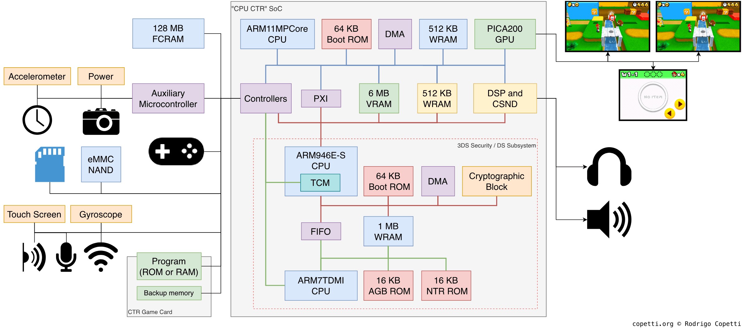
Main diagram of the console's architecture. You can sense that the I/O area on the left side was a strong selling point of this console.
To be fair, we still don't have a standard like USB, but that may be expendable considering the Nintendo 3DS bundles the following:
- A keypad composed of digital buttons, an analogue circle pad.
- 3D and volume sliders.
- A Wi-Fi switch.
- A resistive touch sensor on the bottom screen.
- A gyroscope measuring the console's rotation changes.
- An accelerometer to measure the console's motion.
- One front camera and two back cameras, the latter allowing to take stereoscopic pictures.
- An infrared transceiver, used to transfer data between external accessories.
- An SD card slot, serving as external storage.
- A standard 3.5 mm jack socket for headphones.
- A game card reader, where 3DS, DSi and DS retail games are read from.
The 'New' enhancements
If that wasn't enough, the New 3DS came with more modules on top. This includes:
- Two extra digital buttons and an extra analogue circle pad (called 'C-Stick').
- An NFC Reader on the bottom screen.
- An infrared LED, reserved for head tracking.
- The SD slot is replaced with a microSD slot.
- The Wi-Fi switch has been removed, now it's only controlled through software.
Now, to prevent leaving 'old' users behind, Nintendo provided external accessories to enhance the old models, although most of them relied on the single infrared transceiver to connect. Thus, only one accessory could be connected at the same time.
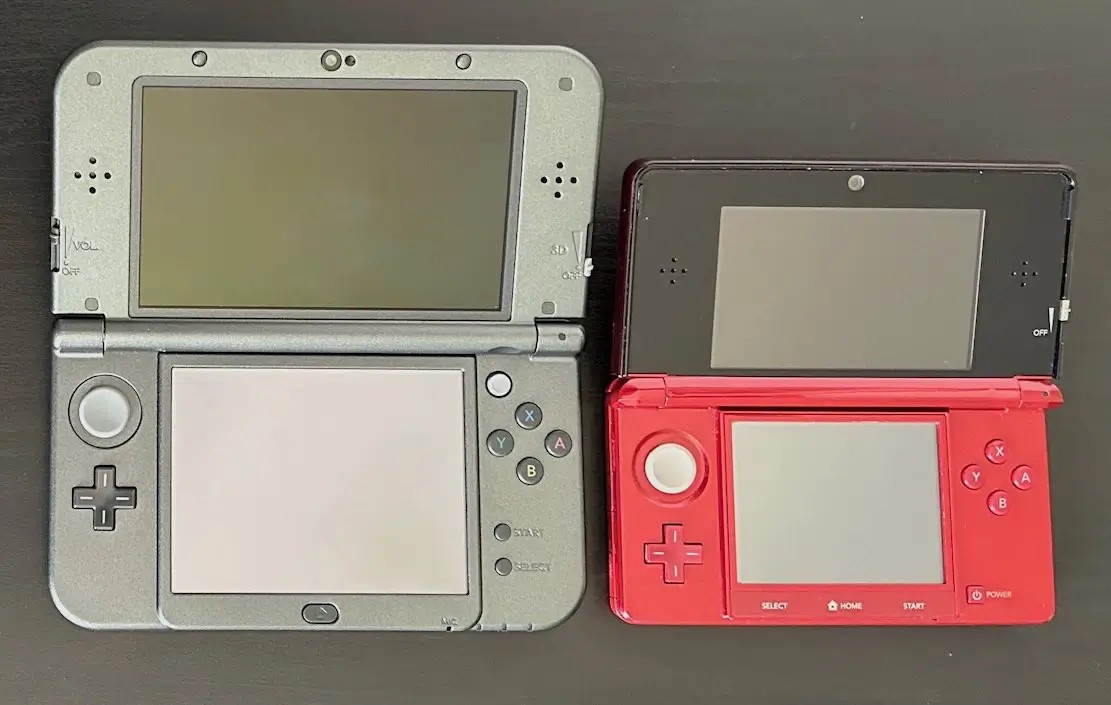
Front view of the New Nintendo 3DS XL and the original 3DS, notice the different button sets each one offers.
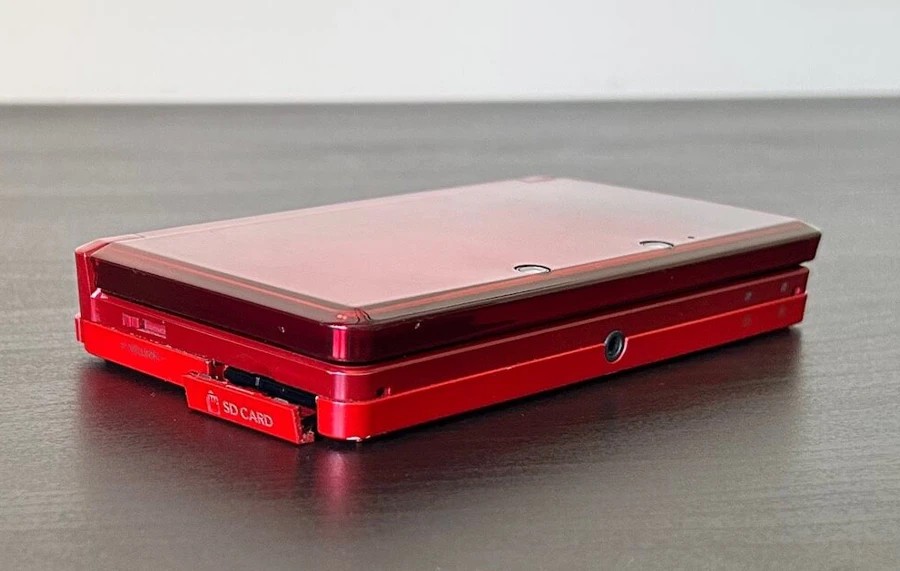
The original 3DS with the SD slot opened. Here you can see the two back cameras, the SD slot and an audio jack port. With the New 3DS, the microSD can't be replaced without taking the back cover off.
Not all the exclusive features of the New 3DS can be replicated, however. For instance, the New 3DS' head tracking mechanism depends on the extra ARM11 core.
Internal interfaces
Now it's time to check how are these interfaces - and others - internally wired up.
Firstly, a large subset is interconnected with the standard Serial Peripheral Interface (SPI) protocol. There are four SPI buses and all of them are accessed by the ARM9 (which I assume also includes the ARM7). The ARM11 only has access to most of them . In any case, the SPI buses connect the following modules :
- The flash memory found inside 3DS game cards, for storing save data.
- DS' Power Management.
- Parts of the Wi-Fi chip.
- Touch screen.
- Sound.
- Microphone.
- Circle Pad.
Curiously enough, some peripherals are interfaced twice to replicate the old DS/DSi's I/O layout and also provide extended capabilities for 3DS software.
Secondly, there's a Human-interface device (HID) module connected to both ARM11 and ARM9 data buses. This is how the digital keypad is accessed. The data is read through a 16-bit register.
Moving on, we got an I²C block which uses a more sophisticated serial protocol. This is connected to the following :
- Front camera, also works in DSi mode.
- Two back cameras, the right camera is accessible in DSi mode as well.
- Infrared transceiver.
- The NFC interface, in the case of the New 3DS.
- The 'QTM' module, used for head-tracking (New 3DS only).
- Gyroscope.
- MCU chip, a separate controller that interfaces more components (explained in the next section).
Finally, there are various registers interfacing FIFO blocks which, in turn, connect to two relatively high-speed (16 MB/s) peripherals :
- Internal eMMC memory.
- SD card slot.
The supplemental computer
As confusing as it may sound, there's more hardware left to discuss. The rest is handled by a middle-man chip called Auxiliary Microcontroller (MCU) . This is just a microcontroller designed by NEC and manufactured by Renesas. Particularly, the model 78K0R, which bundles a proprietary (yet low-power and relatively modern) processor and a ROM . The 78K0R stores a firmware handled by the console's operating system, both ARM9 and ARM11 can interact with it but so do other peripherals.
The MCU chip exclusively controls the following :
- Accelerometer.
- LCD screens.
- LED indicators.
- Power Management.
- Battery fuel gauge and rejection (whether to enable the charging circuitry or not).
- Wi-Fi's EEPROM.
- Real-Time Clock (RTC).
- 3D slider and Wi-Fi switch, the latter is only found on old 3DS models.
- HOME and power buttons.
A subset of this group is already accessible by the main CPUs. This is because the MCU also perform monitoring tasks, thereby saving resources from the ARM11 or ARM9.
Ready for trends
With such a heavy list of I/O hardware, you can now see how Nintendo tried to compete against the smartphone market. This led to interesting services deployed throughout the console's lifecycle:
- A QR Reader bundled with the camera app.
- AR Games: Nintendo shipped 'AR Cards' that could be scanned with the 3DS camera using an app called 'AR Games'. This would make static Nintendo characters pop up in your room, like any traditional augmented-reality-based application.
- Face Raiders: Another camera-based app, but in this case, takes a photo of the player to compose the game's characters. The player must then use the gyroscope and microphone to battle his/her evil clones.
- Amiibos: Uses the NFC reader to scan figurines and unlock game bonuses, the same service was also implemented in the Wii U.
- SpotPass: The continuation of WiiConnect24, now automatically connects to unsecured Wi-Fi access points.
- StreetPass: Automatically exchanges data between nearby 3DS systems. Nintendo marketed it as a way of connecting random 3DS players on the street.
- Play Coins: Unlocks game content by doing some exercise (walking).