Next to a new CPU is always a modern GPU. So, what kind of Picture Processing Unit did Nintendo build this time? To tell the truth, none. For the first time in their portable line, they resorted to a GPU vendor.
Nevertheless, the requirements of Nintendo haven't shifted. The company still wanted a chip with acceptable performance... and the intellectual property core. This will allow them to embed the GPU into their SoC, in the same way they did with the ARM CPUs.
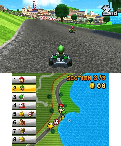
Mario Kart 7 (2011)
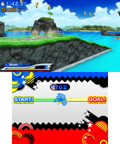
Sonic Generations (2011)
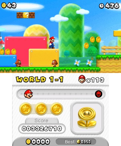
New Super Mario Bros. 2 (2012)
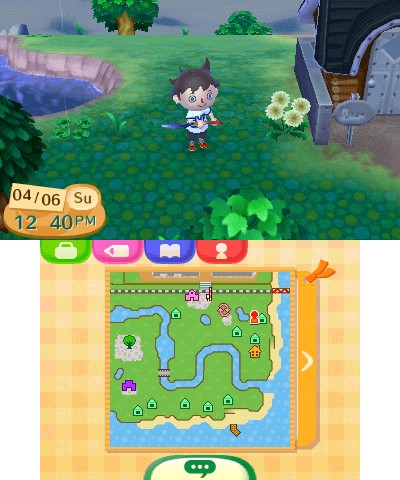
Animal Crossing: New Leaf (2012)
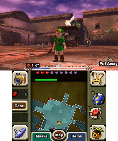
The Legend of Zelda: Majora's Mask 3D (2015)
Meanwhile, a potential candidate just finished unveiling their new invention at SIGGRAPH 2006 . For some time, Digital Media Professionals Inc. (also known as 'DMP') have been building affordable GPUs for the embedded market and, while their chips are nothing out of the ordinary, they guarantee decent OpenGL ES support. Furthermore, their licensing framework offers synthesisable GPUs.
This seemed enough for Nintendo, who happily negotiated a license for DMP's latest core, the PICA200 and subsequently bundled it inside CPU CTR (the Nintendo 3DS' SoC). The GPU runs at 268 MHz.
Architecture of the PICA200
If I had to summarise it in one sentence, the PICA200 is a budget low-power 3D processor that combines a pre-unified architecture with a modernised API. The underlying architecture of the PICA200 is called Maestro 2G and its design is compliant with OpenGL ES 1.1, but extended with elements from OpenGL ES 2.0 . However, the PICA200's APIs are not limited to either standard.
You see, even though the pipeline is segregated and the pixel stage is fixed-function (à la PlayStation 2), DMP expanded the limited circuitry with a set of Maestro functions that provide capabilities beyond the expectations of the embedded market . This includes fragment lighting, multiple shadowing algorithms, polygon subdivision, bump mapping, procedural textures and many fog effects.
Additionally and in contrast to the Nintendo DS, the PICA200 only works with framebuffers. That's it. The sprite engine, a popular workaround to tackle unaffordable memory requirements, is now a thing of the past. This also includes scan-line tricks, as contemporary GPUs work way faster than the refresh rate of a CRT.
Organising the content
Now that we know that this console can draw 3D shapes, the question now is: where does it store its materials? There are two locations, the large FCRAM block and the smaller but faster VRAM.
Nintendo only provided 6 MB of VRAM exclusively for the GPU. Ideally, programmers would fit as much as they can there, but since it will fill up pretty quickly, it is expected to be used to store data that needs instant access (i.e. commands, buffers and recurrent textures) while placing the rest on FCRAM. The PICA200 comes with a DMA unit that can transfer data between FCRAM and VRAM. So, at the end of the day, it's the responsibility of the programmer to come up with an efficient placement to avoid bottlenecks.
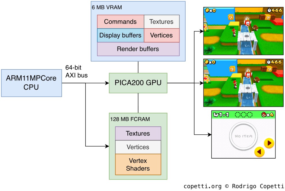
Example of how data is organised across the memory available.
During rendering, programmers allocate dedicated render buffers (i.e. frame, stencil, depth, etc.) for many operations. That's always been the case. With the 3DS, however, the LCD controllers don't understand the data that the PICA200 renders in the frame-buffer. Thus, programmers are also expected to reserve extra space for LCD frame-buffers . Each is bound to a physical screen and encodes the frame in the required format for the LCD controller.
This means that the 3DS is required to allocate at least three LCD frame-buffers (two for the stereoscopic upper screen and one for the bottom one). However, to avoid showing artefacts, a duplicate set may be allocated to perform page flipping.
Based on this, the display process works as follows:
- The LCD continuously displays the content of the active LCD frame-buffer, as instructed by an index register.
- Meanwhile, the GPU finishes rendering new geometry in a separate frame-buffer.
- The frame-buffer is exported to the inactive LCD frame-buffer.
- The GPU swaps the index of the active LCD frame-buffer.
- For practical reasons, the index swap happens at the end of Vertical Sync to avoid tearing down the picture .
- The LCD will now be scanning the recently updated LCD frame-buffer from now on.
Adopting open standards
On an interesting note, just like the ARM11 MPCore adopts ARM's AXI protocol for interconnecting its cores, DMP adopted a less-proprietary option called Open Core Protocol (OCP) . As its name indicates, the Open Core protocol does not impose any licensing restrictions on its users, something that vendors using the PICA200 may find advantageous. For comparison purposes, AXI was released in 2003 (along with the AMBA 3 specification) while OCP was published in 2001. It does make me wonder what kind of technology Nintendo fitted to adapt the OCP signal coming from the PICA200 into an AXI-compliant signal, so the rest of the SoC understands it. I assume that there's a bridge between the PICA200 and the AXI bus.
Interestingly enough, the predecessor of the PICA200, the ULTRAY2000, shares many similarities with its successor. The most notable difference, however, is that the data interfaces use the PCI and DDR-SDRAM protocols instead .
Constructing the frame
Naturally, the GPU is not aware of the stereoscopic or dual-screen nature of the displays, it will only be tasked with rendering three screens during gameplay:
- Top stereoscopic-left: 400 x 240 pixels wide.
- Top stereoscopic-right: 400 x 240 pixels wide.
- Bottom: 320 x 240 pixels wide.
All of them can display 8-bit RGB colours, which equates to up to 16.78 million colours.
Considering players will expect acceptable frame rates on all three screens (especially on the first two), the single PICA200 will be subject to high amounts of workload throughout its operation, an important aspect to remember when judging its performance.
That being said, here is an overview of how data travels to draw a single frame:
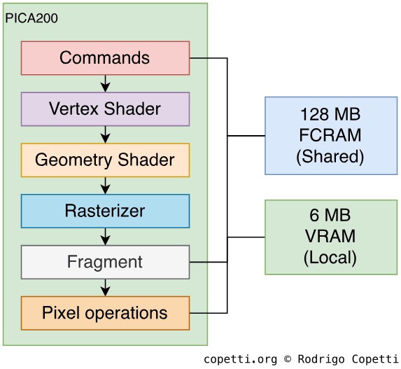
Overview of the graphics pipeline in PICA200.
... and as customary in this series of articles, we'll now take a look at what happens at each stage.
Commands
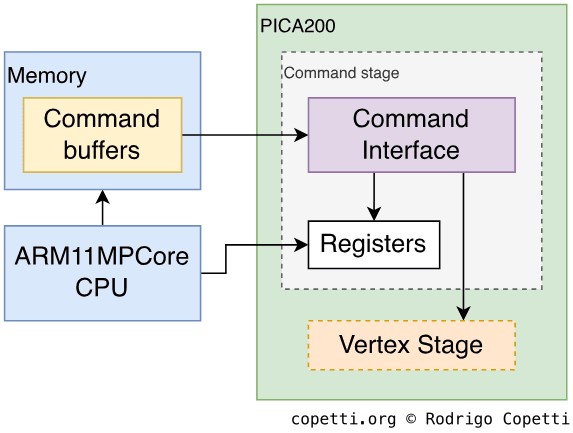
Overview of the command stage.
This is Nintendo's first portable console to finally draw triangles in 'the usual way'. That is, with the use of commands. But it's not a surprising factor, as the PICA200 is expected to abide by the teachings of OpenGL ES.
In essence, the PICA200 draws polygons by reading a command buffer . Furthermore, the vertex data can either be embedded within the command or stored in a separate buffer in VRAM, with the latter being the most efficient.
Vertex
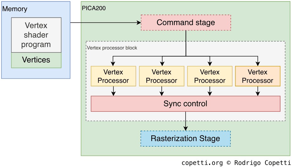
Overview of the vertex stage.
The PICA200 provides four Vertex Processors (VP) that operate in parallel. However, if the geometry shader (the next pipeline stage) is activated, only three processors can be utilised.
Each core computes 96-bit vectors made of four 24-bit floating-point values , but unlike the ARM11's VFP, they don't comply with IEEE-754 . The vertex processors are programmed using assembly language specific to the PICA200 (reminiscent of the days of the Nvidia NV30) and are operated as follows :
- Developers write the vertex shader using PICA200 assembly. For reference, the instruction set is very similar to Microsoft's
vs_2_0. - The shader is compiled using a proprietary assembler.
- The 3DS program must copy the compiled binary to memory (either FCRAM or VRAM).
- Then, the 3DS program issues a GPU command to load the binary and connect it with the program.
Once the vertex cores finish processing, they output the results to the Sync Control block, which acts as a vertex cache and buffer. It has a capacity of 384 Bytes, enabling it to hold up to 32 96-bit vectors. Finally, the next stage reads from this block.
Geometry
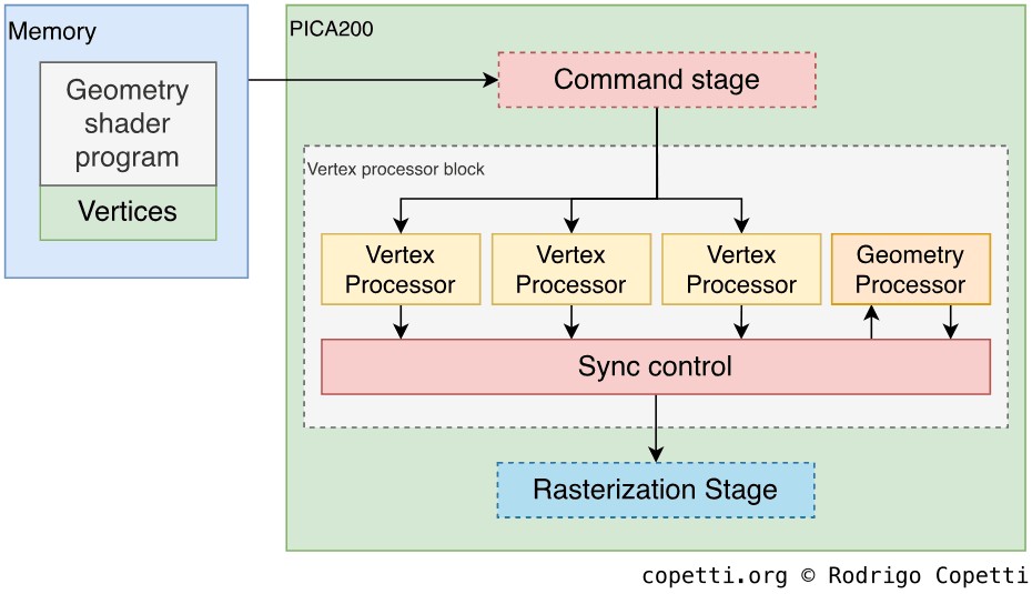
Overview of the geometry stage.
The geometry stage is a signature feature of 8th-generation consoles, allowing developers to spawn complex geometry out of simple vertex data.
In this case, the PICA200's geometry stage is implemented by stealing one of the four Vertex Processors. Then, the 'geometry' vertex core is loaded with a different vertex shader. Finally, it receives the vertex data from the three other processors.
Examples of uses for the geometry shader include square or line generation (using point primitives), geometry subdivision, silhouette edge rendering; and random particle generation.
Rasteriser
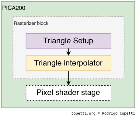
Overview of the rasteriser stage.
At this stage, all primitives are converted into pixels.
The rasterizer unit on the PICA200 is very simple, it just generates triangles out of primitives, then applies culling and clipping to remove unseen triangles (hidden behind others and/or outside the view area, respectively). This is all very similar to OpenGL ES' modus operandi, albeit developers have to watch out for some coordinate systems that are inverted when working with the PICA200.
Fragment
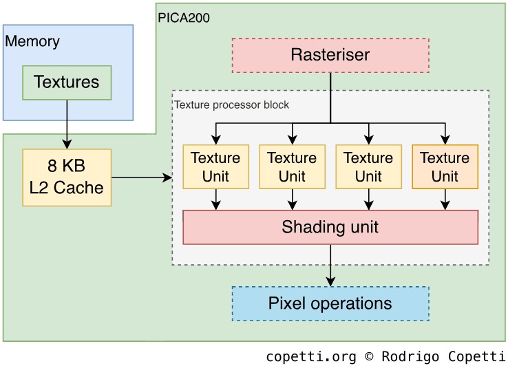
Overview of the fragment stage.
The fragment stage is made of two areas: the texture units, which can fetch textures in memory and process them. And the shading unit, which can perform extra operations on the texture data.
The PICA200 contains four texture units , each houses 256 Bytes of L1 cache and all of them share 8 KB of L2 cache. However, the units are not homogenous. Instead, the range of services varies between each unit :
- Only three units can process 2D textures.
- Only one unit can perform shadow, cube and projective texture mapping.
- The last unit is more of a noise generator, meaning it only outputs random textures. It uses a combination of a random number generator and a colour lookup table. This is a slender yet efficient way of implementing procedure generation with textures, saving bandwidth along the way.
Afterwards, it's the job of the shading unit to creatively fiddle with the textures coming in. However - and something unexpected considering we're talking about an 8th-generation console - is that the PICA200's unit is not programmable with pixel shaders . Instead, we find six configurable colour combiners, each combiner receives three RGB or Alpha values and performs a logical operation on them. The result is passed to the next combiner and so forth. Each colour combiner can get its input from the previous combiner (except the first), a texture unit or a constant value.
All in all, a modern reflection of the Flipper era (while abiding by the OpenGL specification ), but don't forget developers may also combine this with the aforementioned Maestro functions.
Post-processing
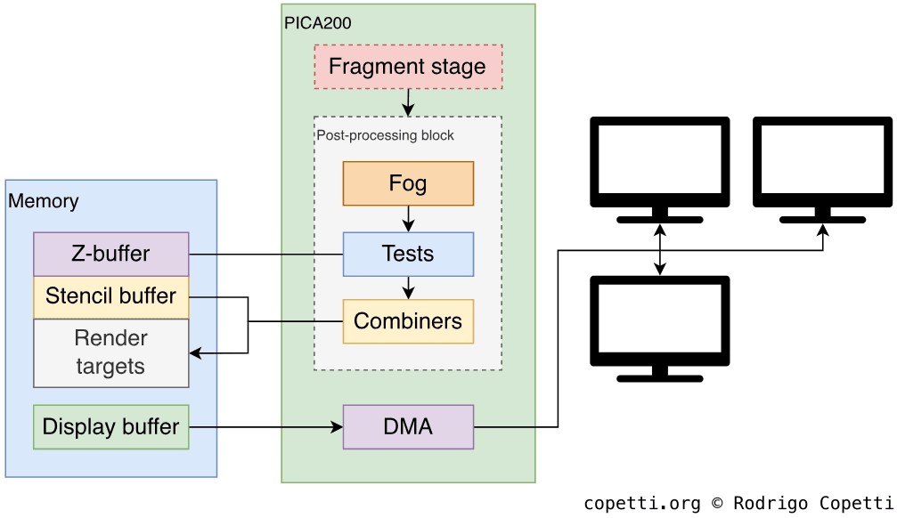
Overview of the post-processing stage.
After the frame is processed and ready to be written into the framebuffer (or render targets), it goes through a sequence of final 'corrections'. This is similar to the OpenGL ES 2.0's pipeline.
That being said, the frame goes through alpha, stencil and depth testing. Afterwards, the result can be mixed with an existing frame (in the framebuffer) using the colour blender or logical operators (AND, XOR, etc.). Finally, the frame is written into the assigned buffer in memory either as a whole or through a stencil filter (for masking).
For additional smoothing of the edges, the PICA200 can render the framebuffer at twice the selected dimensions, and then average it with antialiasing 2x2. This is an old technique known as supersampling.
Once the framebuffer is ready to be displayed, it must be copied into another block in memory called LCD frame-buffer (whose format is better aligned to the scan-line procedure of the LCD screen) and then transferred to the LCD in the form of scan-lines.
Interactive comparison
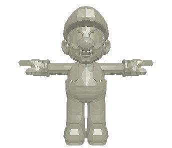
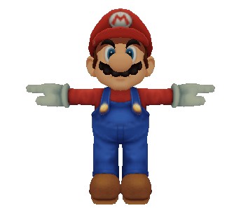
Now that you've seen how the PICA200 draws its triangles on the screen, it's time for some practical examples. Here I've gathered two Marios from Smash Bros games, the Wii and 3DS one. Notice how the perceived level of detail of the newer 'angry Mario' is very close to its home console equivalent.


Interactive model available in the modern edition
Super Smash Bros. Brawl (2008) for the Wii.
5,455 triangles.

Interactive model available in the modern edition
Super Smash Bros. for 3DS (2014).
3,080 triangles.
It's worth reminding again that, in practice, the PICA200 will be rendering three screens at the same time, something that the Wii's GPU wasn't subjected to.
Hidden additions
The 'New' 3DS variant also appears to bundle an uncommon DSP called MVD. It performs H.264 & MJPEG decompression and YUV-to-RGB colour conversion . The CPU programs it by writing to its registers. In turn, the MVD houses a dedicated DMA unit to process the data in FCRAM independently.
Overall, there isn't extensive documentation about this component and I can only presume it resides somewhere in the SoC. The Web Browser found on the New 3DS seems to be its only consumer (for accelerated video playback).
Nostalgic rendering
After all that's been explained, there's one question left unanswered: How does the PICA200 render Nintendo DS and Game Boy Advance games? You may remember that the DS and GBA's GPU exhibit completely different modus operandi for rendering and broadcasting frames.

A frame rendered by the Nintendo DS' Graphics Engine, whose pipeline segregates between 2D and 3D data. That's something the OpenGL-compliant PICA200 doesn't understand.
The explanation is that the DS and GBA PPUs are housed in the SoC and DSi/DS/GBA games will operate them as they originally did on previous consoles. The PPUs output (scanlines) is delivered to a block called LgyFB, which may optionally upscale the frame, and then forward it to the framebuffer, where the PICA200 will take care of displaying it. It's the job of the ARM11 and its DMA to take care of all memory transfers during this process.
Naturally, this arrangement will add some delay (a.k.a. lag), albeit negligible to the user.