Now that we know how the display works, let's look at the internals of this console. If you get a hold of the motherboard, you'll see three big chips, one being the CPU CTR. That's the big System-On-Chip (SoC) that houses the entire system (aside from storage and RAM).
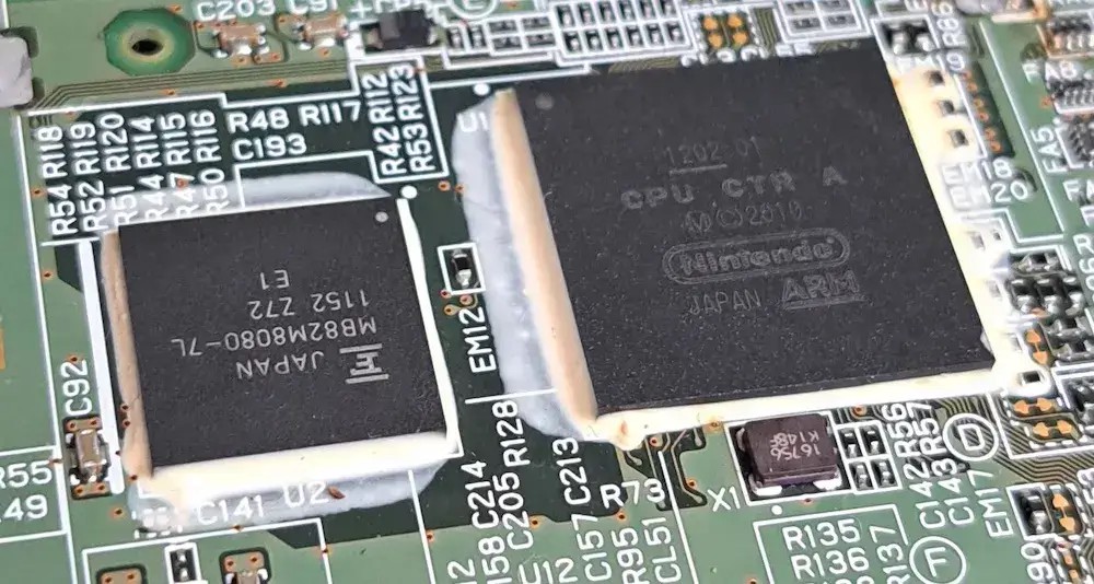
CPU CTR next to some FCRAM
CPU CTR follows the design methods of previous portable consoles from Nintendo. That is, squash all your engineering into a single block. In doing so, it will reduce the production of counterfeits, protect sensible components and improve heat dissipation.
In terms of the actual CPU, Nintendo partnered again with their old friend, ARM, to produce their next-generation core. ARM's traditional licensing model (based on offering synthesisable designs) allows Nintendo to mould a CPU to their needs, including fitting it into a big and opaque SoC. In the end, ARM gave them a relatively antiquated product with substantial upgrades. Their choice was the ARM11, a successor of the ARM9 (featured in the Nintendo DS). More specifically, the MPCore variant, ARM's first homogenous multi-core solution.
Using ARM's designs, Nintendo crafted an ARM11 MPCore cluster housing two ARM11 cores . Three years later, with the arrival of the 'New' 3DS, the SoC was expanded to contain four ARM11 cores. The effects of this will be explained in due time. So, before anything else, let's analyse what the new CPU cores offer to this console.
An iconic industry
The ARM11 series originated in 2002. By then, cellphones ran Java ME applications and bragged about ringtones with actual melodies. In the coming years, the ARM11 became a flagship in the mobile CPU sector, displacing the popular ARM9, the short-lived ARM10 and Intel's XScale. The latter was the continuation of StrongARM, which Intel later sold off to focus on 'low-power' x86 CPUs... if only they knew that the mobile market would skyrocket!
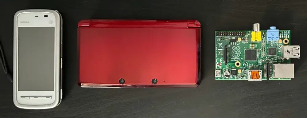
A Nokia 5230 (2009), a red 3DS (2011) and a Raspberry Pi Model B (2012), all carrying an ARM11.
In the end, ARM11s became known for powering the 2006-2009 generation of smartphones. This generation featured a mix of keypad, clamshell and full touchscreen designs. If you owned a Nokia N95, 5230 or the first iPhone, you've used an ARM11. This also applied to many high-end cameras, GPS or similar peripherals. Curiously enough, other manufacturers like RIM and Samsung held onto the Intel XScale until 2009. On a side note, the ARM11 was also the choice of CPU for the first Raspberry Pi.
Now, by the time Nintendo adopted the ARM11, its creator had already succeeded it with the Cortex-A series. This is nothing but expected, as Nintendo's model favours cost-effectiveness over avant-garde CPUs. Look at it from another way, saving in CPU costs allows them to focus their budget on other aspects of the console, you'll soon see.
New dialects...
Along with the new shiny CPUs, a new instruction set arrived, the ARMv6.
From a programmer's perspective, the ARMv6 ISA innovates with a new set of vector instructions and multi-core support . The new vector set is made of SIMD instructions that operate groups of four 8-bit values or two 16-bit values at a time (using the existing 32-bit registers) . These instructions can only operate integers (no floating point), however. Moving on, the new multi-core instructions consist of 'store' and 'load' opcodes with special care for synchronisation (this is crucial when multiple CPUs use the same memory locations) .
All in all, this may not seem that thriving for a new chip series, but remember that ARM's CPUs speak many 'languages'. In the case of an ARM11-based core, you are provided with:
- The main 32-bit ISA, called ARMv6.
- A compressed alternative called Thumb. Its instructions fit in 16-bit words instead. If you'd like to know more, I go over it in the Game Boy Advance and Nintendo DS articles, as it weighs significant importance in those consoles.
- Jazelle, a Java bytecode interpreter, though mostly forgotten and left unused. I've mentioned a bit of it in the Wii article.
- Any extension bundled into the core. For instance, the MPCore includes a Vector Floating-point Coprocessor (VFP) with additional instructions to control said coprocessor . I talk more about this later.
To make matters less confusing, ARM tends to package all of these with a single nomenclature. For instance, in the case of the ARM11 MPCore opcodes, ARM refers to this variant as the ARMv6k instruction set.
... and a fragmented distribution
Be as it may, the adoption of extensions and alternative instruction sets eventually made things very convoluted for developers targeting generic ARM hardware, you only have to look at the uncountable ARM ports devised for Linux distributions.
Debian, one of the most popular distributions, tried to tackle the disparities by developing two ports in parallel:
armel: For wide compatibility (ARMv4T and onwards).armhf: Accelerated with the VFP extension, but only compatible with ARMv7 onwards.
Yet, with the arrival of the Raspberry Pi (powered by ARMv6 and accelerated with the VFP), neither of them was deemed acceptable. Thus, an unofficial port called 'Raspbian' was developed to provide a VFP-accelerated version for ARMv6 CPUs . Even so, the trend continued: years later, with the arrival of ARMv8 and AArch64, Debian spawned yet-another port, arm64, optimised for the new 64-bits ISA.
I don't remember seeing this labyrinth with x86 (even though the adoption of x86 SIMD extensions hasn't been consistent, to say the least), but at least things are now getting more orderly. AArch64 has unified many extensions and dropped alternative modes (farewell, Thumb and Jazelle).
Core functionality
... That was a quick detour, let's go back to analysing what's in the 3DS CPU!
For this study, we can divide the ARM11 MPCore into two areas:
- The MP11 cores that make up the cluster.
- The Advanced eXtensible Interface (AXI) bus, a new invention that interconnects the cores and interfaces with the outside world.
Let's start with the cores now and then we'll check the AXI bus.
The original MPCore
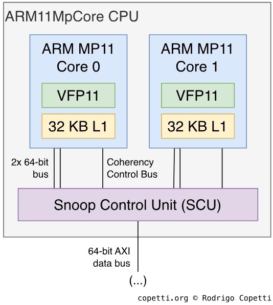
Overview of the ARM11 MPCore CPU cluster
The first ARM11 MPCore variant, which debuted with the original 3DS, includes two cores. Each is called MP11 and runs at 268 MHz .
Apart from implementing the ARMv6k instruction set, the MP11 features an 8-stage pipeline and it's complemented with two levels of branch prediction: 'dynamic' (based on previous executions) and 'static' (based on the current instruction alone). Overall, I sense these new additions are part of a new design philosophy that will eventually obsolete the iconic conditional execution, although we won't notice this until the next generation.
Additionally, since the ARM946E-S CPU, ARM has been fitting a System Control Coprocessor called CP15. This time, it provides Memory-Management (MMU functions) and register memory that output information about the MPCore cluster.
Now, there's no more Tightly-Coupled Memory (TCM). There are however 16 KB of instruction cache and 16 KB of data cache, this change of model resembles other systems of the same generation. If you are curious, this L1 cache is 4-way set associative.
Finally, each core houses a co-processor called Vector Floating-point Coprocessor (also known as 'VFP', or 'VFP11' in the case of the ARM11). This accelerates arithmetic operations with floating-point numbers, both 32-bit single-precision (a.k.a. float) and 64-bit double-precision (a.k.a. double) ones . It's not a big coprocessor though, as its register file is composed of thirty-two 32-bit registers, so doubles will consume two registers. In any case, this processor implements the VFPv2 instruction set and follows the IEEE 754 standard. The latter is a welcomed decision, considering the difficulties of previous generations.
The 'New' MPCore

Overview of the 'New' CPU cluster
With the arrival of the New 3DS in 2014, a new SoC was included (CPU LGR) and with it, a luxurious CPU upgrade.
The most apparent change is that we have now four MP11 cores instead of two. The consequences of this, however, are not simple to disseminate, but we'll see them in due time.
The second change is that the CPU incorporates 2 MB of L2 cache shared between the four cores. This type of cache is 16-way associative, which anticipates four cores accessing it at the same time. If you'd like to know more, I went over associative caches with the Xbox 360 article.
Moving on, all cores now run at 804 MHz (three times the original speed, which will certainly raise a few eyebrows).
The AXI bus
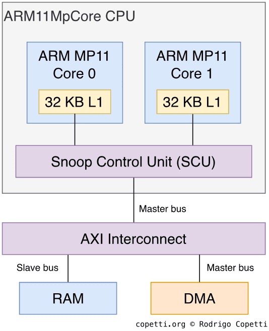
Example of the Nintendo 3DS' AXI implementation interconnecting different types of components. Here, the CPU and DMA act as masters while the RAM node is the slave. However, the roles can change as deemed fit.
Whether we're talking about two or four MP11 cores, all of these are connected using a popular bus, proudly authored by ARM, called the Advanced eXtensible Interface (AXI). This protocol is part of the AMBA3 model, a successor of the original AMBA revision that we've seen in the Wii and Wii U (both housing an ARM9 CPU). In doing so, ARM offered the AXI model as a critical building block for System On Chips (SoC).
Generally speaking, the AXI model provides a set of protocols for connecting components with distinct bandwidth requirements. These are free to choose any particular topology, like the token-ring model of the PlayStation 3 or the mesh solution made for the Xbox 360. Now, within the Nintendo 3DS, we find a combination of bus and star designs.
Following AMBA's methodologies for interconnecting nodes, there will be a master-slave hierarchy to denote which entity is in charge. The master components (typically, the CPU cores) will be the ones sending commands to the slaves (i.e. memory and I/O blocks).
Furthermore, the AXI network can be arbitrated using a dedicated block (called AXI interconnect) acting as a bus matrix . This is what we find in the MPCore and relies on individual 64-bit buses . In doing so, the network tackles the congestion of high-bandwidth components (something that consoles like the PlayStation 2 struggled with). Moreover, multiple master devices can communicate with slave nodes using separate channels to avoid waiting for other masters to finish. And if that's not enough, traditional enhancements like burst transactions are also implemented, from which the MP11 cores take advantage.
In the case of the 3DS, the AXI interconnect is housed in a bigger block called Snoop Control Unit (SCU) that also takes care of automatically maintaining L1 cache coherency between the MP11 cores.
Any other CPUs?
Up to this moment, I've been talking about the MPCore as if it were the only CPU in this system, the reason being mixing up distinct CPUs for this analysis can turn it into an incomprehensible essay. That is, until now.
The truth is, Nintendo had extra requirements for this console. They wanted a proper security system, but also the possibility to turn the console into a Nintendo DSi or a GBA on-the-fly. So, for all of that, they ended up bundling three distinct CPU packages - one being the mentioned ARM11. The other two are well hidden, in the sense that games are completely unaware of them. In fact, 3DS emulators like Citra don't care about them at all .
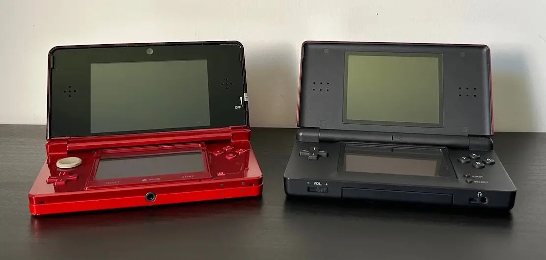
The Nintendo 3DS next to a predecessor (a Nintendo DS Lite), the latter has become a common denominator.
But we do! So here's the complete list of the CPUs this system houses:
- The ARM11 MPCore we've just seen.
- An ARM946E-S from the Nintendo DS days. It's treated as a secret co-processor and it's only managed by the operating system. Alternatively, it becomes the main processor whenever a DS or DSi game is executed.
- Thanks to its bundled CP15 co-processor, there's a Memory Protection Unit (MPU) in place. This will protect the CPU from arbitrarily executing code from any location in memory.
- An ARM7TDMI from the Game Boy Advance days. It's a relatively ignored CPU, unless a DS or DSi game is being played, in which case it acts as a co-processor. However, on the special occasion when a Game Boy Advanced game is running, the main execution falls into this CPU.
Unfortunately, or for obvious reasons, the three CPUs are never usable at the same time. Instead, the console has three modes of operation:
- Native 3DS mode: The ARM11 MPCore executes a 3DS game while the ARM946E-S deals with I/O and security. The ARM7, on the other side, is switched off.
- Nintendo DSi mode: The ARM946E-S and ARM7TDMI operate in a multi-processor configuration to execute a Nintendo DS or DSi game. Just like with its predecessor, the ARM7TDMI has greater access to I/O. Meanwhile, the ARM11 MPCore will be working in the background to replicate missing and re-located DS hardware (real-time clock, power management, keypad, GBA/DS PPU display and so forth).
- Game Boy Advance mode: The ARM7TDMI is the only CPU executing instructions (in 99% of cases, that will come from a GBA game). The ARM11 MPCore and ARM9, both still operating within the capacities of 'Native 3DS mode', will be working in the background.
If you stop to think about it, the Nintendo 3DS ends up housing four processors in total (Two MP11 cores + one ARM9 + one ARM7), or the absurd amount of six in the case of the New 3DS. How convoluted is that? Luckily, this system didn't suffer the complications of the Sega Saturn and you can thank Nintendo and ARM's engineering for that. After all, 3DS developers only had to deal with the MPCore.
Since the ARM9 and ARM7 are predominantly for I/O, security and backwards compatibility (neither of which require the developer's awareness), I discuss them in later sections of this article. But if you'd like to know more about the design of the ARM7 and ARM9, I wrote about them in previous articles (the Game Boy Advance and Nintendo DS ones, respectively).
Multi-core communication
I guess the question now is, how can CPUs and cores talk to each other? Well, the easiest way is to share RAM... but you could also try a more efficient approach, depending on the cores trying to communicate:
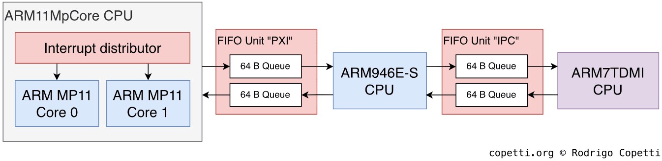
Representation of the communication channels each CPU is provided with.
- With inter-core ARM11 communication, a core can send interrupts to another core by writing on its
Software Interrupt Register. - In the case of ARM11<->ARM9 or ARM9<->ARM7 communication, the same FIFO model from the Nintendo DS is implemented. Plus, the ARM11<->ARM9 FIFO is also called 'PXI' .
Memory available
Having three different CPUs also means the memory layout will not be simple, especially if you care about security.
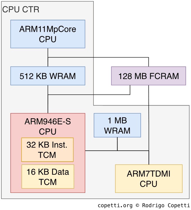
Overview of memory organisation on the Nintendo 3DS.
To make a long story short, we've got the following blocks:
- From the developer's perspective, the system provides 128 MB of FCRAM. The New 3DS increased this to 256 MB. The rest is redundant for games.
- For predominantly security reasons, the ARM11 is also provided with a fast block of 512 KB of SRAM. The ARM9 is also given a block of 1 MB of SRAM (1.5 MB in the case of the New 3DS).
- By inheriting the model of the Nintendo DS, the ARM9 also houses Tightly-Coupled Memory (TCM). Particularly, there's 32 KB for instructions and 16 KB for data.
A new type of memory spotted
It's all jolly that the Nintendo 3DS includes 32 times the general-purpose memory of its predecessor, but what's that 'FCRAM'? Is it any different from the other standards?
Well, Fast Cycle DRAM (FCRAM) is yet another RAM invention, this time authored in 2002 by Fujitsu and Toshiba. Presented as an alternative to DRAM-based technology (i.e. SDRAM, EDO DRAM, RDRAM, etc.), FCRAM excels on non-continuous reads, where it exhibits a lower latency than DRAM . This was done to replicate the performance offered by the more expensive SRAM.
FCRAM competes directly with DDR DRAM by offering a revamped design of the memory arrays. In place of adding more circuitry on top of it, arrays are split into smaller subblocks, which are then accessed using a 3-stage pipeline . In doing so, reading and writing on random locations become faster. These changes are still designed with backwards compatibility in mind. Thus, FCRAM is compatible with DDR DRAM controllers (hence, its full name is 'DDR FCRAM').
Faster memory transfers
The inventors of the MPCore and the AMBA bus happen to also offer a brand of DMA controllers called CoreLink, with Nintendo being a loyal client. So, it's no mystery as to why the 3DS bundles multiple blocks of CoreLink DMA-330 into their SoC .
These DMAs in particular are attached to an AXI bus and act as master devices. Each can transfer data between two slaves interconnected with the AMBA protocol (either AXI or the slower APB) .
Nintendo fitted one CoreLink DMA next to the ARM9, this is referred to as XDMA and provides up to four channels (thus, up to four concurrent transfers). There's another DMA next to the ARM11 block, this time called CDMA, which provides up to eight channels. With the arrival of the New 3DS, another CoreLink DMA-330 is fitted next to the ARM11 block (now a quad-core cluster).
Programming
With all being said, how do you program a system featuring this unorthodox CPU arrangement? To be fair, unusual systems are no strangers to videogame developers. But in this case, 3DS programmers only have access to the ARM11 MPCore. Furthermore, once you reach the 'Operating System' section, you'll learn the abilities with this cluster are further restricted.
In any case, no matter the console revision, programmers base their algorithms on the multi-threading model: the program groups sequences of instructions using threads, these are then dispatched by the operating system to the physical cores, as the former deems fit. Once a novelty for Xbox 360 software, this standard provides a layer of abstraction that blinds the developers from writing software only compatible with a fixed number and type of CPU cores.
Dealing with the 'New' hardware
Since the New 3DS diverts considerably from the original specification, Nintendo set up a thin compatibility layer to enable old 3DS games to work with the new hardware without manual intervention.
In essence, when a game is launched from a New 3DS console, the game's code specifies if it's specifically targeting the new models or not . If it is, the operating system will proceed to activate all the novelties (faster clock speed, extra RAM and use of L2 cache) for that game to enjoy. If it's not, the operating system will keep its exclusive hardware deactivated until the user exits the game, so the game can safely assume it's running on the old hardware and will do so without issue.
To keep supporting the old 3DS, games can be packaged with two codebases (one for the 'New' model and the other for the 'Old' one). It's up to the game studios to decide whether to support the old and new 3DS, or only the new 3DS.
You may be wondering what happens with the rest of the exclusive hardware the New 3DS houses (i.e. extra ARM11 cores and DMA). Well, to properly understand the rationale, I explain this once you reach the 'Operating System' section, but I'm afraid you won't like the answer!